

MOS power device and manufacturing method thereof
A manufacturing method and technology of power devices, applied in semiconductor/solid-state device manufacturing, semiconductor devices, electric solid-state devices, etc., can solve problems such as high manufacturing cost, unstable performance parameters, and large size of MOS-type power devices
- Summary
- Abstract
- Description
- Claims
- Application Information
AI Technical Summary
Problems solved by technology
Method used
Image


Examples
Embodiment Construction
[0034] Specific embodiments of the present invention will be described in detail below in conjunction with the accompanying drawings. It should be understood that the specific embodiments described here are only used to illustrate and explain the present invention, and are not intended to limit the present invention.
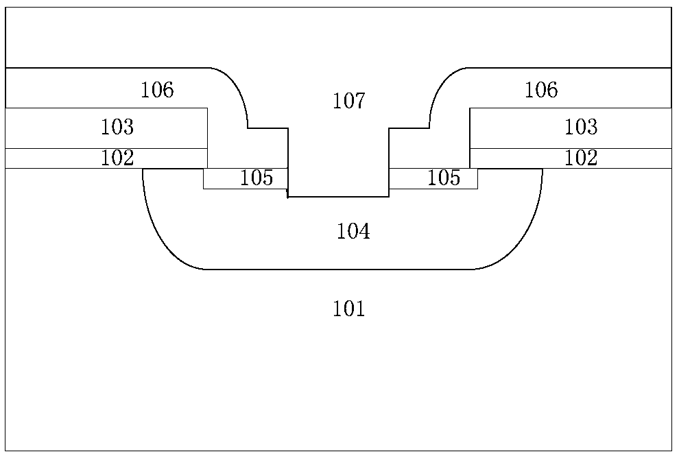
[0035] Embodiments of the present invention will now be described with reference to the drawings, in which like reference numerals represent like elements. Combined with reference below image 3 and Figures 3a-3i The manufacturing method of the MOS type power device of the present invention will be described in detail. image 3 A flow chart of a method for manufacturing a MOS power device provided by an exemplary embodiment of the present invention. Such as image 3 As shown, the method may include the following steps.
[0036] Step S101: sequentially forming the first insulating dielectric layer 302, the first semiconductor layer 303, the second insulatin...
PUM
 Abstract
Description
Claims
Application Information