Silicon nitride optical waveguide device and graphene detector integrated chip and manufacturing method thereof

A waveguide device, silicon nitride light technology, applied in the directions of optical waveguide light guide, light guide, optical components, etc., can solve the problems of high cost and difficult process, achieve wide electrical bandwidth, wide light absorption wavelength range, and simple device structure. Effect

Active Publication Date: 2018-06-29
NO 55 INST CHINA ELECTRONIC SCI & TECHNOLOGYGROUP CO LTD
View PDF8 Cites 19 Cited by
  • Summary
  • Abstract
  • Description
  • Claims
  • Application Information

AI Technical Summary

Problems solved by technology

[0004] The present invention proposes a silicon nitride optical waveguide device and a graphene detector integrated chip and its manufacturing method, and its purpose is to address the difficulty and high cost of the existing indium phosphide detector and silicon-based optical waveguide device integrated chip process problem, it is proposed to adopt the method of integrating graphene detector and silicon nitride-based optical waveguide device, in which the silicon nitride optical waveguide device processes the optical signal, and the graphene detector performs photoelectric conversion on the processed optical signal, so as to realize a single On-chip integrated optical signal processing functional unit and chip

Method used


Image

  • Silicon nitride optical waveguide device and graphene detector integrated chip and manufacturing method thereof
  • Silicon nitride optical waveguide device and graphene detector integrated chip and manufacturing method thereof
  • Silicon nitride optical waveguide device and graphene detector integrated chip and manufacturing method thereof

Examples


Embodiment

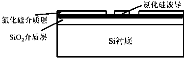
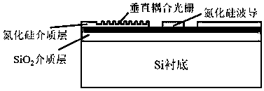
[0045] A silicon nitride optical waveguide device and graphene detector integrated chip, its structure includes a silicon nitride vertical coupling grating 1, a silicon nitride optical waveguide device 2 and a graphene detector 3; wherein the silicon nitride vertical coupling grating is an optical The signal input port is connected to the A multimode interference coupler 6A in the silicon nitride optical waveguide device 2, the silicon nitride optical waveguide device 2 processes the optical signal, and passes through the B multimode interference coupler in the silicon nitride optical waveguide device 2 The coupler 6B is connected and transmits the processed optical signal to the graphene detector 3, and the graphene detector 3 performs photoelectric conversion on the processed optical signal.

[0046] The silicon nitride vertical coupling grating 1 has a grating period of 1.1 microns, a duty cycle of 50%, and an etching depth of 300 nanometers.

[0047] Described silicon nitr...


PUM


Abstract

The invention discloses a silicon nitride optical waveguide device and graphene detector integrated chip and a manufacturing method thereof. The integrated chip structurally comprises a silicon nitride vertical coupling optical grating, a silicon nitride optical waveguide device and a graphene detector, wherein the silicon nitride vertical coupling optical grating is an optical signal input port,and is connected to the silicon nitride vertical coupling optical grating; the silicon nitride optical waveguide device is used for processing an optical signal, the processed optical signal is connected and transmitted to the graphene detector, and the graphene detector is used for carrying out photovoltaic conversion on the processed optical signal. The integrated chip has the advantages that firstly, various reconfigurable optical signal processing functions can be realized by designing the silicon nitride optical waveguide device with different structure; secondly, compared with a traditional indium phosphide based detector, the graphene detector has boarder optical absorption wavelength range and wider electrical bandwidth; and thirdly, the device is simple in structure, and an optical signal processing function unit and a chip of on-chip monolithic integration can be realized.

Description

technical field [0001] The invention relates to a silicon nitride optical waveguide device and a graphene detector integrated chip and a manufacturing method, belonging to the technical field of integrated microwave optical signal processing. Background technique [0002] Photon technology has outstanding advantages such as wide bandwidth, low transmission loss, anti-electromagnetic interference, and tunability. The combination of photon technology and radio frequency microwave technology has produced microwave photon technology. By modulating radio-frequency microwave signals on lasers, functions such as signal generation, modulation, processing, and long-distance low-loss transmission can be realized at optical frequencies. It is a key technology leading the future communication industry and military fields such as radar and electronic warfare. Microwave photon signal processing is one of the research hotspots. At present, many photon signal processing functions have been ...

Claims


Application Information

Patent Timeline
Patent Type & Authority Applications(China)
IPC IPC(8): H01L27/142G02B6/12
CPCG02B6/12004G02B2006/12138G02B2006/12176H01L27/142Y02E10/50
Inventor 顾晓文吴云牛斌曹正义
Owner NO 55 INST CHINA ELECTRONIC SCI & TECHNOLOGYGROUP CO LTD
Why Eureka
Try Eureka