
Display panel and manufacturing method thereof

A manufacturing method and display panel technology, which can be applied in the directions of instruments, nonlinear optics, optics, etc., can solve problems such as the influence of the performance of liquid crystal devices and the unclean cutting of PI substrates.

Active Publication Date: 2021-03-23
WUHAN CHINA STAR OPTOELECTRONICS TECH CO LTD
View PDF11 Cites 0 Cited by
  • Summary
  • Abstract
  • Description
  • Claims
  • Application Information

AI Technical Summary

Problems solved by technology

[0005] Usually, in the basic manufacturing process of flexible liquid crystal display devices, after the cell forming process is completed, each liquid crystal cell needs to be cut separately, and the glass substrates on the CF (color film) side and the Array (array) side are peeled off, and then The process of polarizing the polarizer, bonding the chip and the flexible circuit board (IC&FPC bonding), and assembling the backlight module, among which the cutting process mainly adopts the cutter wheel cutting process in the traditional liquid crystal display device manufacturing process, and the cutter wheel needs to be on the glass substrate. However, the PI substrate has a certain degree of flexibility and the PI substrate and the glass substrate have limited adhesion. Therefore, the cutting edge of the PI substrate is likely to be unclean due to the cutting edge of the PI substrate, thus affecting the liquid crystal device. Performance has a fatal impact

Method used


Image

  • Display panel and manufacturing method thereof
  • Display panel and manufacturing method thereof
  • Display panel and manufacturing method thereof

Examples


Embodiment Construction

[0024] Hereinafter, embodiments of the present invention will be described in detail with reference to the accompanying drawings. This invention may, however, be embodied in many different forms and should not be construed as limited to the specific embodiments set forth herein. Rather, the embodiments are provided to explain the principles of the invention and its practical application, thereby enabling others skilled in the art to understand the invention for various embodiments and with various modifications as are suited to particular intended uses.

[0025] In the drawings, the thicknesses of layers and regions are exaggerated for clarity. Like reference numerals refer to like elements throughout the drawings.

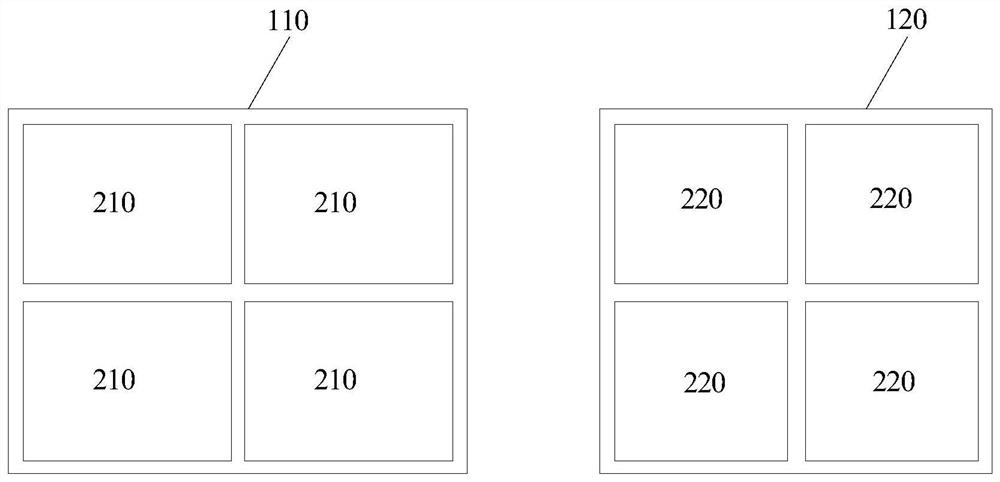
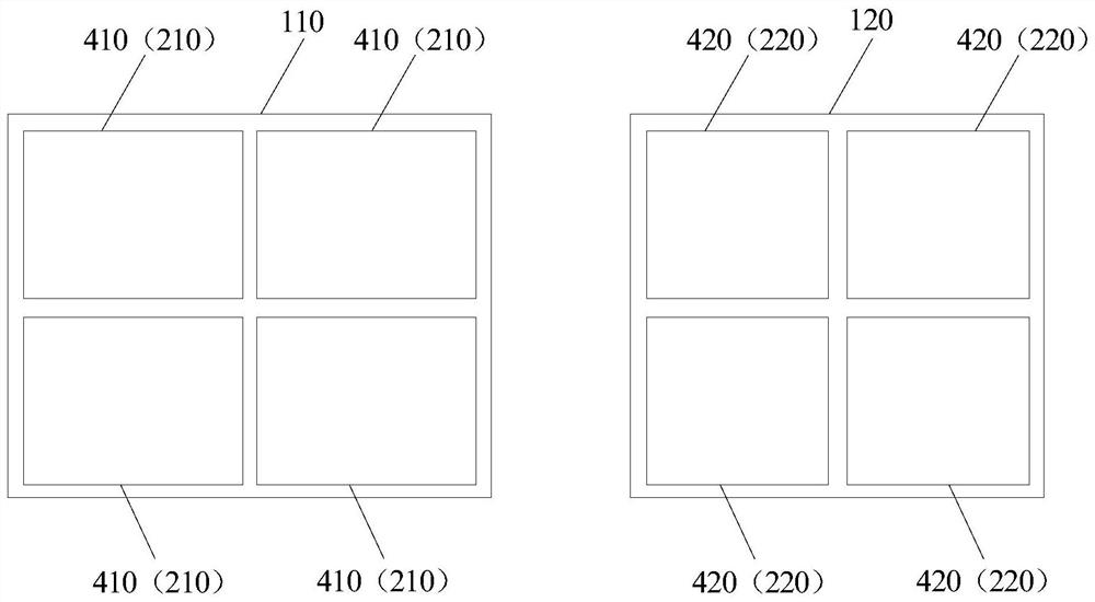
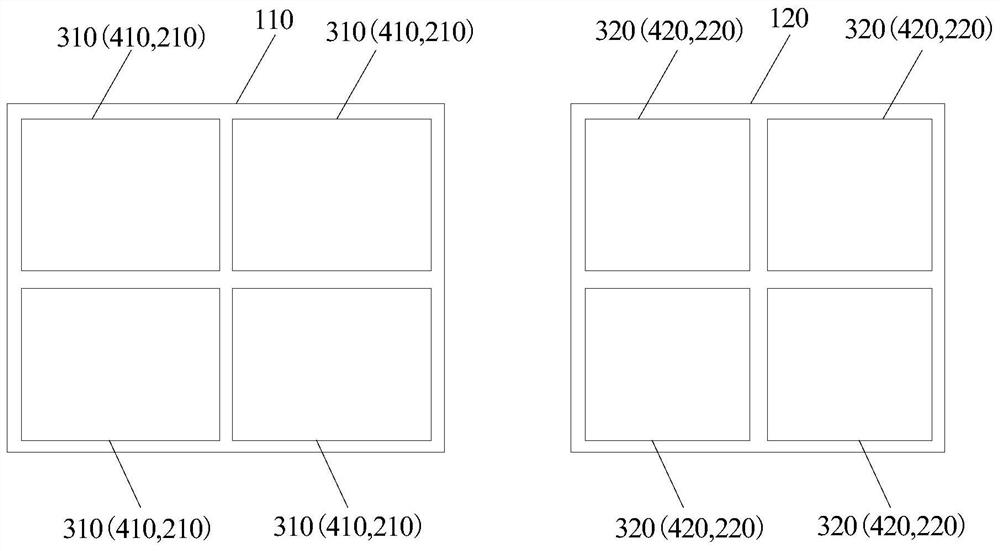
[0026] Figure 1A to Figure 1F is a process diagram of a display panel according to an embodiment of the present invention. figure 2 is a flowchart of a method for manufacturing a display panel according to an embodiment of the present invention.

[0027] refe...


PUM


Abstract

The invention provides a manufacturing method of a display panel. The manufacturing method comprises steps as follows: multiple patterned first flexible substrates are formed on a first rigid substrate, and multiple patterned second flexible substrates are formed on a second rigid substrate; an array process is completed on each first flexible substrate to form multiple array areas, and a color film process is completed on each second flexible substrate to form multiple color film areas; the array areas and the color film areas are in one-to-one correspondence to form multiple liquid crystal boxes; the liquid crystal boxes are cut and separated along boundaries of the first flexible substrates and the second flexible substrates; the first rigid substrate and the first flexible substrates of the liquid crystal boxes are lifted off, and the second rigid substrate and the second flexible substrates of the liquid crystal boxes are lifted off. The flexible substrates matched with the shapesof the liquid crystal boxes independently are formed in advance, during cutting, the liquid crystal boxes are cut and separated along the boundaries of the flexible substrates, and accordingly, the phenomenon of incomplete cutting of the morphology of cutting edges of the flexible substrates can be prevented.

Description

technical field [0001] The invention belongs to the technical field of display panel manufacturing, and in particular relates to a display panel and a manufacturing method thereof, in particular to a flexible display panel and a manufacturing method thereof. Background technique [0002] With the gradual rise of wearable application devices such as smart glasses and smart watches, the demand for flexible display devices in the display industry is also increasing. Organic light emitting diode (Organic Light Emitting Display, OLED) display has the characteristics of self-illumination without backlight, thin thickness, wide viewing angle, fast response speed, etc., so it has the natural advantages of flexible display. However, the current OLED industry still has a high technical threshold, difficult manufacturing process, low yield, high cost, and high price. These difficulties hinder the wide application of OLED. [0003] Liquid Crystal Display (LCD) has a relatively long dev...

Claims


Application Information

Patent Timeline
Patent Type & Authority Patents(China)
IPC IPC(8): G02F1/1333
CPCG02F1/1333G02F1/133305G02F1/133351
Inventor 崔宏青查国伟
Owner WUHAN CHINA STAR OPTOELECTRONICS TECH CO LTD
Learn More