High-k dielectric trench lateral double-diffused metal oxide element semiconductor field effect transistor and method of making the same
A lateral double-diffusion, field effect transistor technology is applied in the field of lateral double-diffusion metal oxide element semiconductor field effect transistors and their fabrication
- Summary
- Abstract
- Description
- Claims
- Application Information
AI Technical Summary
Problems solved by technology
Method used
Image
Examples
Embodiment Construction
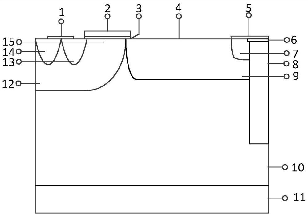
[0043] Such as figure 1 As shown, the high-K dielectric trench lateral double-diffused metal oxide element semiconductor field effect transistor of the present invention includes:
[0044] A substrate 11 of elemental semiconductor material (such as silicon or germanium) (the doping concentration of the substrate is 1×10 13 cm -3 ~1×10 15 cm -3 );
[0045] an epitaxial layer 10 grown on a substrate 11;
[0046] A base region 12 and a drift region 9 formed on the epitaxial layer 10;
[0047] A source region 13 and a channel 15 formed on one side of the base region 12 adjacent to the drift region 9, and a drain region 7 formed on the other side of the drift region 9;
[0048] a channel substrate contact 14 formed outside the source region 13 in the base region;
[0049] The source electrode 1 formed by shorting the contact surface between the source region and the channel substrate;
[0050] A gate insulating layer 3 and a gate electrode 2 formed corresponding to the chan...
PUM
| Property | Measurement | Unit |
|---|---|---|
| relative permittivity | aaaaa | aaaaa |
Abstract
Description
Claims
Application Information
