A three-dimensional light source structure

A technology of three-dimensional light source and epitaxial structure, applied in semiconductor devices, electric solid-state devices, electrical components, etc., can solve the problems of heat dissipation, lack of red part, poor color rendering, etc., to reduce environmental pollution and improve light output capability.

Active Publication Date: 2020-04-14
SHENZHEN GUANGMAO ELECTRONICS
View PDF4 Cites 0 Cited by
  • Summary
  • Abstract
  • Description
  • Claims
  • Application Information

AI Technical Summary

Problems solved by technology

[0002] At present, there are three common processes for realizing white LEDs in production as follows: YAG phosphor is excited on the blue LED chip, and the yellow-green light and blue light it emits are synthesized into white light. However, the spectrum of white light emitted by this technology is missing The red part has poor color rendering, and it is difficult to meet the lighting requirements of low color temperature; using RGB three-color multiple chips or multiple devices to emit light and mix colors into white light, or use blue and yellow dual-chip complementary colors to produce white light, although this method can be passed Select the appropriate wavelength and intensity to obtain a better color rendering index, but the difference in chip performance makes the drive circuit too complicated and heat dissipation becomes a problem; apply RGB phosphor powder on the ultraviolet light chip, and use purple light to excite the phosphor powder to produce three primary colors. Forms white light, however, due to the low efficiency and high cost of current UV chips and RGB phosphors, this technology has not yet reached the practical stage

Method used


Image

  • A three-dimensional light source structure
  • A three-dimensional light source structure
  • A three-dimensional light source structure

Examples


Embodiment Construction

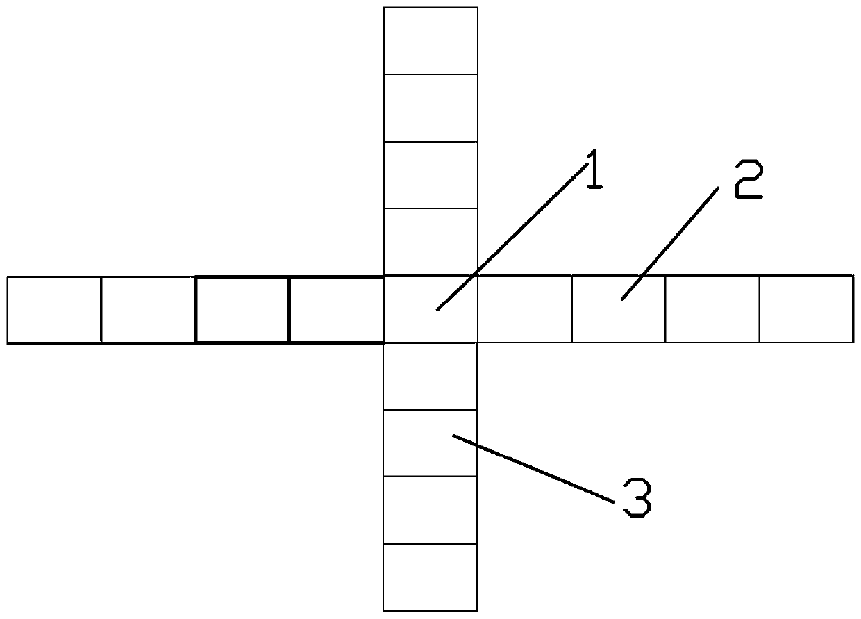
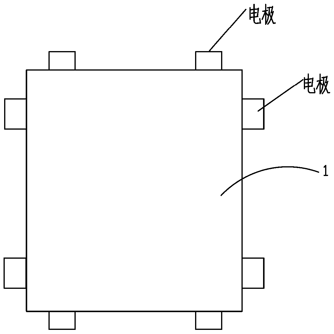
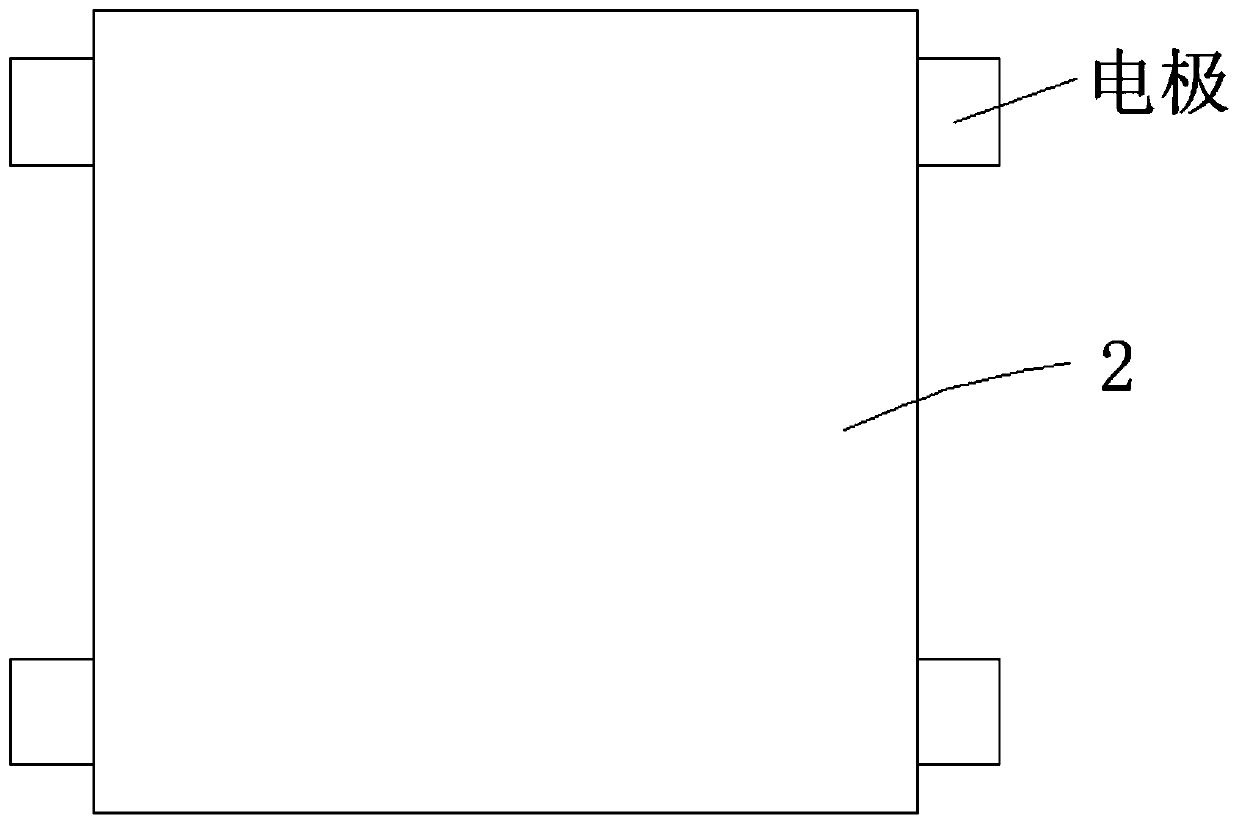
[0029] In order to facilitate the understanding of the present invention, reference will be made to the relevant appended Figure 1-5 The present invention is described more fully. Preferred embodiments of the invention are shown in the accompanying drawings. However, the present invention can be embodied in many different forms and is not limited to the embodiments described herein. On the contrary, the purpose of providing these embodiments is to make the disclosure of the present invention more thorough and comprehensive.

[0030] Unless otherwise defined, all technical and scientific terms used herein have the same meaning as commonly understood by one of ordinary skill in the technical field of the invention. The terminology used herein in the description of the present invention is only for the purpose of describing specific embodiments, and is not intended to limit the present invention. As used herein, the term "and / or" includes any and all combinations of one or mo...


PUM

PropertyMeasurementUnit
thicknessaaaaaaaaaa

Abstract

A novel three-dimensional light source structure includes a center chip, a horizontal chip, and a vertical chip, wherein the horizontal chip and the vertical chip are respectively connected to the center chip, electrodes between the horizontal chip and the center chip are correspondingly connected by the zinc chip, electrodes between the vertical chip and the center chip are correspondingly connected by the zinc chip, each of the center chip, the horizontal chip and the vertical chip are rectangular in cross section, and the lower surfaces are respectively provided with an epitaxial structure;P electrodes and N electrodes are respectively disposed around the center chip; P electrodes and N electrodes are respectively disposed on the left side surface and the right side surface of the horizontal chip; and P electrodes and N electrodes are respectively disposed on the upper side surface and the lower side surface of the vertical chip.

Description

technical field [0001] The invention relates to the field of semiconductor lighting, in particular to a three-dimensional light source structure. Background technique [0002] At present, there are three common processes for realizing white LEDs in production as follows: YAG phosphor is excited on the blue LED chip, and the yellow-green light and blue light it emits are synthesized into white light. However, the spectrum of white light emitted by this technology is missing The red part has poor color rendering, and it is difficult to meet the lighting requirements of low color temperature; using RGB three-color multiple chips or multiple devices to emit light and mix colors into white light, or use blue and yellow dual-chip complementary colors to produce white light, although this method can be passed Select the appropriate wavelength and intensity to obtain a better color rendering index, but the difference in chip performance makes the drive circuit too complicated and he...

Claims


Application Information

Patent Timeline
Patent Type & Authority Patents(China)
IPC IPC(8): H01L25/075H01L33/48H01L33/62H01L33/64H01L33/06H01L33/12
CPCH01L25/0753H01L33/06H01L33/12H01L33/48H01L33/62H01L33/641
Inventor 李锋吉爱华叶浩文
Owner SHENZHEN GUANGMAO ELECTRONICS
Why Eureka
Try Eureka