Method for fabricating light emitting diode

A technology of light-emitting diodes and manufacturing methods, which is applied in the direction of electrical components, circuits, semiconductor devices, etc., and can solve problems such as poor heat dissipation, high manufacturing cost, and long growth time

Active Publication Date: 2009-04-08
EPISTAR CORP
View PDF4 Cites 0 Cited by
  • Summary
  • Abstract
  • Description
  • Claims
  • Application Information

AI Technical Summary

Problems solved by technology

However, this method must grow a very thick light-transmitting substrate, thus making the growth time too long and making the manufacturing cost higher
In addition, since the AlGaAs substrate has the same disadvantage of poor heat dissipation as the GaAs substrate, it is not suitable for operation at high currents
[0004] Another disadvantage of AlGaAs epiwafer is that its surface often has ripple or terrace stripes and bends, which makes the subsequent grain manufacturing process more difficult
[0005] Therefore, it is necessary to have a method for manufacturing light-emitting diodes, which can convert the epitaxial wafers of light-emitting diodes from substrates with poor thermal conductivity to substrates with good thermal conductivity when the surface of the epitaxial wafers of light-emitting diodes is uneven or curved, so as to improve Heat dissipation characteristics of light-emitting diodes and solve the problem of substrate light absorption

Method used


Image

  • Method for fabricating light emitting diode
  • Method for fabricating light emitting diode
  • Method for fabricating light emitting diode

Examples


Embodiment Construction

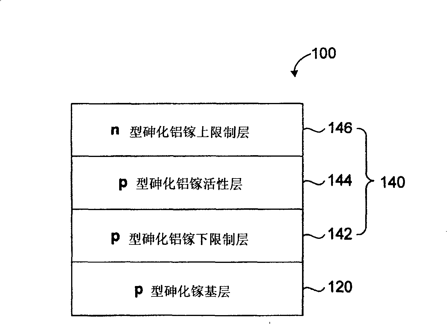
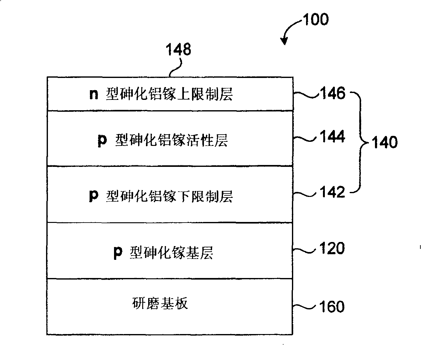
[0013] The present invention discloses a light emitting diode 10 (shown in Image 6 ) method of manufacture. In an embodiment according to the present invention, a light-emitting diode is manufactured by using an AlGaAs epitaxial wafer grown by a liquid phase epitaxial growth method. The aluminum gallium arsenide epitaxial wafer 100, which is generally grown by the liquid phase epitaxial growth method, has the advantage of low cost, such as figure 1 shown. The AlGaAs epitaxial wafer 100 has a first substrate 120 and an epitaxial layer 140 , and the epitaxial layer 140 includes a lower confinement layer 142 , an active layer 144 and an upper confinement layer 146 . refer to figure 1 , the aluminum gallium arsenide epitaxial wafer 100 in this embodiment is a double heterostructure (double heterostructure, DH) red light emitting diode epitaxial wafer, the wavelength is about 660nm, and it has a p-type gallium arsenide substrate 120, p Type AlGaAs lower confinement layer 142 (...


PUM


Abstract

Polycrystalline chip of light emitting diode (LED) is provided first. The chip of LED includes first base plate and polycrystalline layer. Surface of polycrystalline layer of the chip is evened. At least an ohmic contact layer is formed on part of the evened surface. Metal light reflection layer is formed to cover the ohmic contact layer and polycrystalline chip of LED. Barrier to diffusion layer is formed on the metal light reflection layer. Second base plate is jointed to the barrier to diffusion layer, and then first base plate is removed.

Description

technical field [0001] The invention relates to a method for manufacturing a light-emitting diode, in particular to a method for manufacturing a light-emitting diode using a commercial light-emitting diode epitaxial wafer grown by a liquid phase epitaxial growth method. Background technique [0002] At present, the epitaxial layer of aluminum gallium indium phosphide (AlGaInP) light-emitting diodes grown by metal organic vapor phase epitaxy (MOVPE) has a wavelength range up to 645nm. The epitaxial layer of light-emitting diodes with a wavelength greater than 645nm (mainly infrared and red light-emitting diodes of aluminum gallium arsenide) is mainly grown by liquid phase epitaxy (LPE). [0003] The aluminum gallium arsenide (AlGaAs) epitaxial wafer grown by the liquid phase epitaxial growth method not only has a relatively high output power, but also has a relatively low cost. However, the gallium arsenide substrate absorbs light, which leads to the disadvantage of poor lum...

Claims


Application Information

Patent Timeline
Patent Type & Authority Patents(China)
IPC IPC(8): H01L33/00
Inventor 陈泽澎谢素芬
Owner EPISTAR CORP
Why Eureka
Try Eureka