Circuit board and electronic device provided with same

一种电路基板、贯通孔的技术,应用在电路热装置、电路、印刷电路等方向,能够解决散热特性降低、接合面积小、接合不良等问题,达到减小凹陷、提高散热特性、提高接合强度的效果

Inactive Publication Date: 2014-02-12
KYOCERA CORP
View PDF5 Cites 8 Cited by
  • Summary
  • Abstract
  • Description
  • Claims
  • Application Information

AI Technical Summary

Problems solved by technology

However, in the case of forming a via conductor by filling it with metal plating, since the metal plating grows from the inner wall of the via hole, a depression is formed in the center of the surface of the via conductor.
Also, when the metal paste is filled, a depression occurs in the center of the surface of the through conductor due to shrinkage during firing.
Furthermore, since the surface shape of the metal wiring layer formed to cover the surface of the through conductor conforms to the surface shape of the through conductor, depressions also occur on the surface of the metal wiring layer. When electronic components are mounted on a chip or the like, there is a problem that poor bonding occurs between the members, and the heat dissipation characteristics decrease due to the small bonding area.

Method used


Image

  • Circuit board and electronic device provided with same
  • Circuit board and electronic device provided with same
  • Circuit board and electronic device provided with same

Examples


Embodiment 1

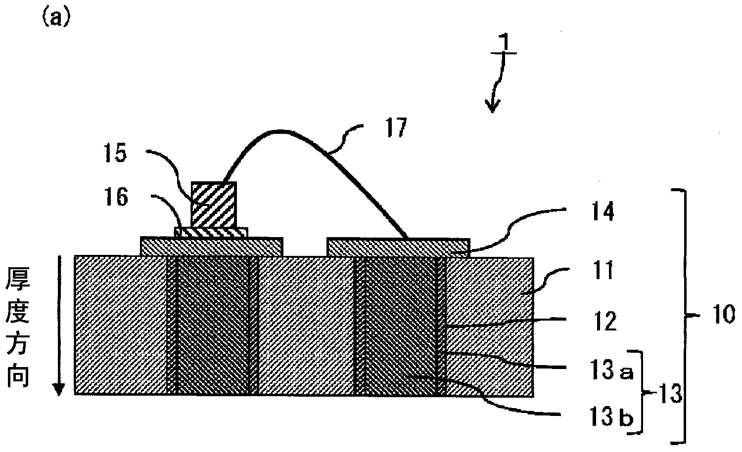
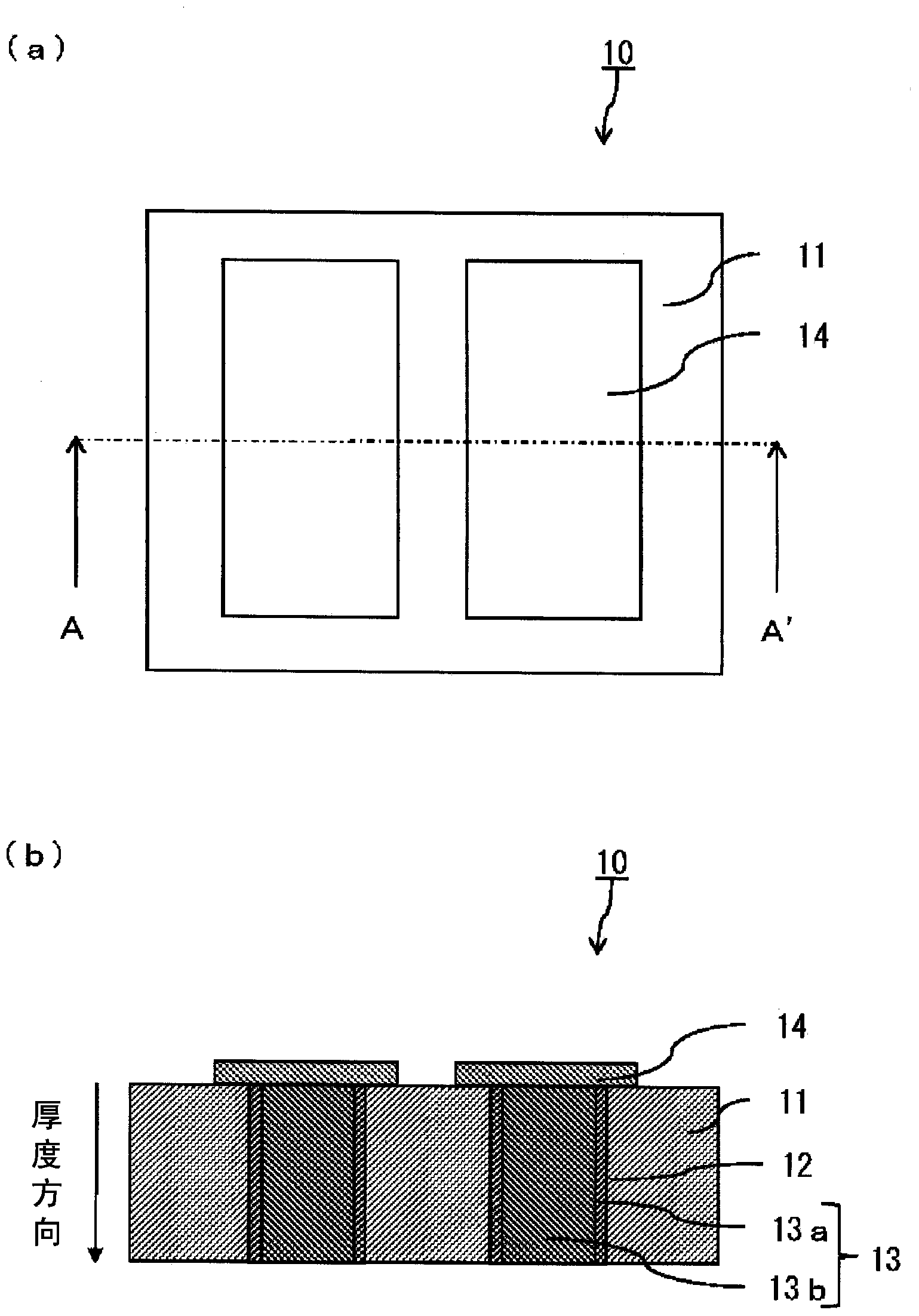
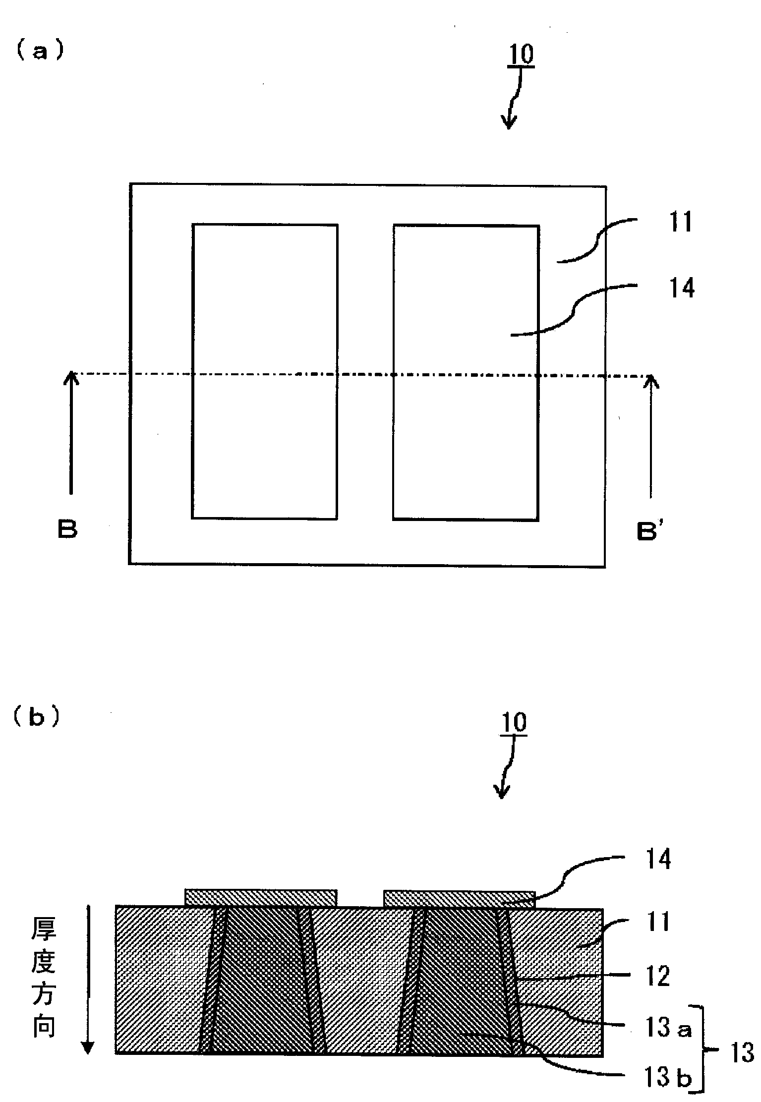
[0067] Samples were produced in which the average crystal grain diameters of the first region 13 a and the second region 13 b were different, and tests were performed on the dishing, heat dissipation characteristics, and reliability of the via conductor 13 .

[0068] First, using silica and magnesia as sintering aids, an alumina-based sintered body having an alumina content of 96% by mass was produced. It should be noted that groove processing is performed on the ceramic sintered body 11 so that a plurality of samples can be obtained.

[0069] Then, laser processing was performed on the ceramic sintered body 11 to form a through-hole 12 having a diameter of 130 μm from one end to the other end. Next, for the metal pastes used to prepare the samples, those made of copper and having an average particle size of 0.5 μm, 2 μm, and 6 μm in the mixing ratio of metal powders were used to obtain the average crystal grain size shown in Table 2. The way to adjust the metal mixed powder ...

Embodiment 2

[0082] Next, samples were produced in which the second region 13b of the penetrating conductor 13 and the average crystal grain size of the metal wiring layer 14 were different, and tests regarding heat dissipation characteristics and reliability were performed. As a manufacturing method, in order to make the average crystal grain size of the metal wiring layer 14 different on the penetrating conductor 13 having the same structure as sample No. 14 of Example 1, Sample Nos. 4, 8, and 14 to form the metal wiring layer 14 using the metal paste used in the formation of the second region 13b. It should be noted that the structure of the metal wiring layer 14 is the same as the second region 13b of the sample No. 4 of Example 1 is the sample No. 19, and the same as the sample No. 14 is the sample No. 20. The same as sample No.8 is sample No.21. Except changing the metal paste used, it carried out by the same method as Example 1.

[0083] Furthermore, a heat dissipation characteris...

Embodiment 3

[0088] Next, samples were produced in which the glass content in the first region 13a was different from the glass content in the second region 13b, and tests regarding heat dissipation characteristics and reliability were performed. As a manufacturing method, the mixing ratio of the second metal paste was changed, the glass powder of sample No. 22 was changed to 2.0% by mass, the glass powder of sample No. 23 was changed to 3.0% by mass, and the The glass powder was changed to 4.0% by mass. In addition, the ratio of terpineol to acrylic resin was fixed at 3.4, and the addition amount of the organic vehicle was increased / decreased according to the amount of glass powder. The same method as in Example 1 and Example 2 was carried out except that the second metal paste used was changed.

[0089] The heat dissipation characteristic test and the heating cycle test were performed by the same method as in Example 1. In the method of measuring the glass content in the first region 1...


PUM

PropertyMeasurementUnit
softening pointaaaaaaaaaa
particle diameteraaaaaaaaaa

Abstract

The invention provides a highly-reliable circuit board and an electronic device obtained by mounting electronic components on the circuit board, which have high bonding strength and excellent heat discharge properties, and can be used over a long period as a result of minimizing cavities in a metal wiring layer formed on a through conductor. A circuit board (10) is provided with a through conductor (13) comprising a metal in a through hole (12) that penetrates in the thickness direction of a ceramic sintered body (11), and a metal wiring layer (14) that covers and is connected to the surface of the through conductor (13) on at least one main surface side of the ceramic sintered body (11). The through conductor (13) comprises: a first area (13a) that is positioned on an inner wall side of the through hole (12), from one end to the other end of the through hole (12) in the thickness direction of the ceramic sintered body (11); and a second area (13b) that adjoins the first area (13a). The average crystal grain size in the second area (13b) is larger than the average crystal grain size in the first area (13a).

Description

technical field [0001] The present invention relates to a circuit board and an electronic device formed by mounting electronic components on the circuit board. Background technique [0002] Electronic devices in which various electronic components such as semiconductor elements, heating elements, and Peltier elements are mounted by bonding to metal wiring layers on a circuit board are used. These electronic components generate heat during operation, and since the heat per unit volume applied to the circuit board has increased due to the high integration of electronic components and the miniaturization and thinning of electronic devices in recent years, a bonding method has been sought. A circuit board that does not peel off and has high heat dissipation characteristics. [0003] For this reason, in the support substrate constituting the circuit board, a through-hole is formed at a position directly below the electronic component, and the heat radiation characteristic is imp...

Claims


Application Information

Patent Timeline
Patent Type & Authority Applications(China)
IPC IPC(8): H05K1/11H01L23/13H01L23/14H05K1/09
CPCH05K1/0206H01L2224/73265H05K2201/0266H01L23/3677H05K1/09H05K2201/0326H05K3/4061H01L2924/13091H05K1/0306H05K1/115H01L23/15H01L2924/13055H05K2203/049H01L23/49827H01L2924/12032H01L2924/1305H01L2224/32225H01L2224/48091H01L2224/48227H01L2924/00H01L2924/00014H01L2924/00012
Inventor 中村清隆大桥嘉雄阿部裕一平野央介四方邦英关口敬一
Owner KYOCERA CORP
Why Eureka
Try Eureka