Deposition device and depositon method

A technology for deposition devices and substrates, which is applied in the fields of electrical components, semiconductor/solid-state device manufacturing, circuits, etc., can solve the problems of reduced deposition accuracy and distortion of thin film patterns, and achieve the effects of improving accuracy and reducing sagging

Active Publication Date: 2017-05-31
SAMSUNG DISPLAY CO LTD
View PDF6 Cites 19 Cited by
  • Summary
  • Abstract
  • Description
  • Claims
  • Application Information

AI Technical Summary

Problems solved by technology

This misalignment results in reduced deposition accuracy and thus can cause distortions in the pattern of the thin film formed by depositing the deposition species on the substrate

Method used


Image

  • Deposition device and depositon method
  • Deposition device and depositon method
  • Deposition device and depositon method

Examples


Embodiment Construction

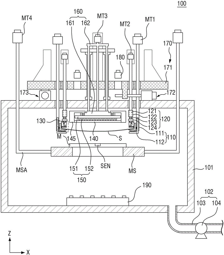
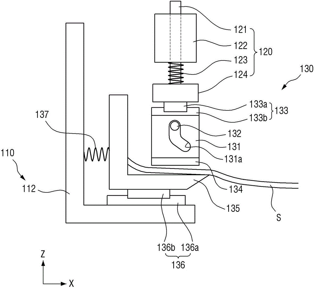
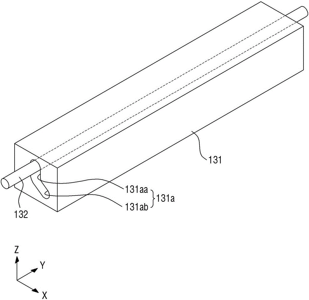
[0048] Advantages and features of the present invention and methods for achieving the advantages and features will be clarified with reference to the embodiments described in detail below with reference to the accompanying drawings. However, the present invention is not limited to the embodiments disclosed below, but can be realized in various forms different from each other. These embodiments are provided only to make the disclosure of the present invention complete and to fully inform those skilled in the art to which the present invention pertains, and the present invention is defined only by the scope of the claims.

[0049] When an element or layer is referred to as being "on" another element or layer, the element or layer is directly on the other element or layer or with the other layer or other element interposed therebetween. The same reference numerals denote the same constituent elements throughout the specification.

[0050] It should be clear that although first, ...


PUM


Abstract

The invention provides a deposition device and a deposition method. As a typical example, the deposition device comprises multiple substrate bearing parts, multiple substrate clamping parts, multiple stretching blocks and multiple pushing rods. The substrate bearing parts bear two end parts of a substrate and are configured to be capable of moving in a rising and descending manner. The substrate clamping parts and the two end parts of the substrate are arranged on each of the substrate bearing part and are configured to be capable of moving in a rising and descending manner. The stretching blocks are arranged between the substrate bearing parts and the substrate clamping parts respectively and horizontally move in a way of being away from each other when the substrate clamping parts move in the descending manner, thereby stretching the substrate. The pushing rods are capable of moving in a rising and descending manner, arranged in the stretching blocks respectively and allow the stretching blocks to horizontally move in a way of being away from each other through the descending moving.

Description

technical field [0001] The invention relates to a deposition device and a deposition method. Background technique [0002] Liquid crystal display devices, plasma display devices, organic light emitting display devices, and the like are widely used as display devices. [0003] Such a display device can be manufactured by depositing a deposition substance on a substrate by a deposition process to form a thin film. [0004] To form a thin film on a substrate, the end of the substrate is supported to expose the deposition face of the substrate during the deposition process. However, since the substrate is upsized as the display device is upsized, severe sagging occurs in the central portion of the substrate. In this case, errors may occur during the alignment of the substrate and the mask. Such misalignment results in reduced deposition accuracy and thus may cause distortion in the pattern of the thin film formed by depositing the deposition substance on the substrate. Cont...

Claims


Application Information

Patent Timeline
Patent Type & Authority Applications(China)
IPC IPC(8): H01L21/683H01L21/687H01L21/02
CPCH01L21/02104H01L21/6831H01L21/687
Inventor 李炳哲金盛来西口昌男车裕敏郑成镐
Owner SAMSUNG DISPLAY CO LTD
Why Eureka
Try Eureka