Electronic component package and method for producing same

A technology for electronic components and manufacturing methods, which is applied in semiconductor/solid-state device manufacturing, electrical components, and electrical solid-state devices, etc., can solve problems such as insufficient connection reliability of heat dissipation characteristics, and achieve the effect of improving connection reliability.

Inactive Publication Date: 2015-04-29
PANASONIC INTELLECTUAL PROPERTY MANAGEMENT CO LTD
View PDF8 Cites 8 Cited by
  • Summary
  • Abstract
  • Description
  • Claims
  • Application Information

AI Technical Summary

Problems solved by technology

[0011] However, the conventional technology has insufficient heat dissipation characteristics and connection reliability in high-density mounting.

Method used


Image

  • Electronic component package and method for producing same
  • Electronic component package and method for producing same
  • Electronic component package and method for producing same

Examples


Embodiment

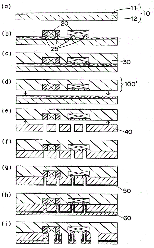
[0112] The electronic component package of the present invention was produced as follows.

[0113] Materials used in the production of the electronic component package of the present invention are as follows.

[0114] 1. Adhesive carrier (adhesive film): Adhesive single-sided tape (adhesive layer about 15 μm + polyester film about 200 μm) about 200mm×about 200mm

[0115] 2. Sealing resin layer: liquid epoxy resin

[0116] 3. Metal foil: single-sided glossy copper foil (about 18μm) / roughened surface on the resin side

[0117] An electronic component package was manufactured according to the following steps.
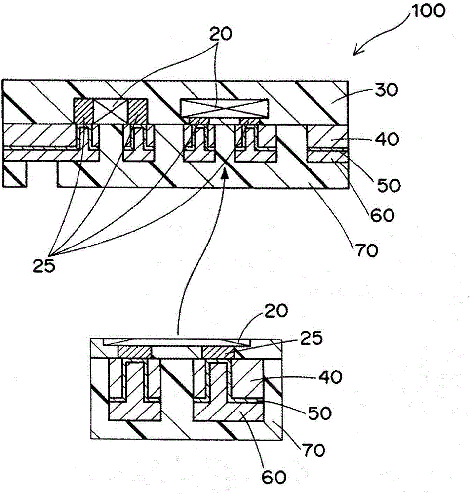
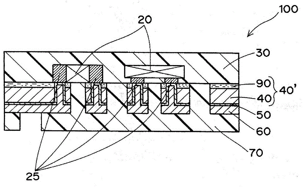
[0118]

[0119]

[0120] Since the metal foil 40 constituting the metal wiring layer is in direct contact with the sealing resin layer 30 through the above steps, and the metal plating layer constituting the metal wiring layer is in direct contact with the electrode 25 of the electronic component 20, the heat from the electronic component can be suppressed. The he...


PUM

PropertyMeasurementUnit
thicknessaaaaaaaaaa
thicknessaaaaaaaaaa
thicknessaaaaaaaaaa

Abstract

This method for producing an electronic component package comprises: (i) a step wherein a package precursor, in which an electronic component is embedded in a sealing resin layer such that an electrode of the electronic component is exposed from the surface of the sealing resin layer, is formed; (ii) a step wherein a metal foil having a through hole is provided on the surface of the sealing resin layer such that the through hole is at a position where the through hole faces the electrode of the electronic component; and (iii) a step wherein a metal plating layer is formed on the metal foil. In step (iii), the metal plating layer is formed by performing a wet plating process after performing a dry plating process and the through hole of the metal foil is filled with the metal plating layer, so that the metal plating layer and the metal foil are integrated with each other.

Description

technical field [0001] The present invention relates to an electronic component package and a method of manufacturing the same. In more detail, this invention relates to the package provided with the electronic component, and its manufacturing method. Background technique [0002] Along with the development of electronic equipment, various mounting techniques have been developed in the field of electronic technology. As examples, there is a mounting technology (packaging technology) using a circuit board or a lead frame as a mounting technology (packaging technology) for electronic components such as ICs and inductors. That is, there are "a package using a circuit board" and a "package using a lead frame" as a package form of a general electronic component. [0003] "Packages Using Circuit Substrates" (Reference Figure 5 (a)) It has the form which mounted the electronic component on the circuit board. As the type of this package, generally there are "wire bonding type (W...

Claims


Application Information

Patent Timeline
Patent Type & Authority Applications(China)
IPC IPC(8): H01L23/12H01L23/02H01L33/62H01L33/64
CPCH01L33/62H01L33/52H01L33/647H01L2933/0066H01L24/19H01L2224/48091H01L2924/19105H01L2224/04105H01L2224/92144H01L23/367H01L23/3677H01L23/3735H01L2924/12041H01L23/3107H01L23/3121H01L21/561H01L21/565H01L21/568H01L24/96H01L2924/12042H01L2924/181H01L2224/16225H01L2224/16245H01L2224/73265H01L2924/00014H01L2924/00H01L2924/00012H01L21/56H01L21/76877H01L23/28H01L23/34H01L23/50
Inventor 一柳贵志中谷诚一山下嘉久
Owner PANASONIC INTELLECTUAL PROPERTY MANAGEMENT CO LTD
Why Eureka
Try Eureka