1.55-micron-wavelength silicon-based quantum dot laser epitaxial material and preparation method thereof

A technology of silicon-based quantum dots and epitaxial materials, used in lasers, phonon exciters, laser parts, etc., can solve the problems of unfavorable silicon-based optoelectronic integration, long growth time of epitaxial materials, etc., to reduce the growth time of materials, improve Material growth quality, the effect of reducing lattice mismatch

Inactive Publication Date: 2020-09-04
JIANGSU HUAXING LASER TECH CO LTD
View PDF0 Cites 7 Cited by
  • Summary
  • Abstract
  • Description
  • Claims
  • Application Information

AI Technical Summary

Problems solved by technology

However, this method of transition through the buffer layer will make the part of the laser active region structure to the substrate too thick, which is not conducive to silicon-based optoelectronic integration, and makes the growth time of laser epitaxial materials too long

Method used


Image

  • 1.55-micron-wavelength silicon-based quantum dot laser epitaxial material and preparation method thereof
  • 1.55-micron-wavelength silicon-based quantum dot laser epitaxial material and preparation method thereof
  • 1.55-micron-wavelength silicon-based quantum dot laser epitaxial material and preparation method thereof

Examples


Embodiment Construction

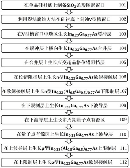
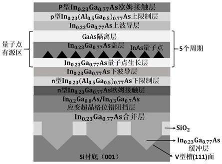
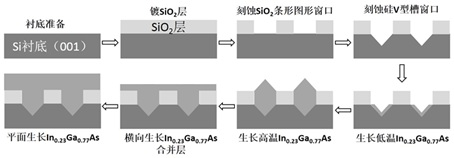
[0039] In order to make the objectives, technical solutions, and advantages of the present invention clearer, the following further describes the present invention in detail with reference to the accompanying drawings and specific embodiments. It should be understood that the specific embodiments described here are only used to explain the present invention, but not to limit the present invention.

[0040] In the following, many aspects of the present invention will be better understood with reference to the drawings. The parts in the drawings are not necessarily drawn to scale. Instead, the focus is on clearly describing the components of the invention. In addition, in several views in the drawings, the same reference numerals indicate corresponding parts.

[0041] The word "exemplary" or "illustrative" as used herein means serving as an example, instance, or illustration. Any embodiment described herein as "exemplary" or "illustrative" is not necessarily construed as being pre...


PUM

PropertyMeasurementUnit
thicknessaaaaaaaaaa
thicknessaaaaaaaaaa
thicknessaaaaaaaaaa

Abstract

The invention relates to the technical field of semiconductor lasers, in particular to a 1.55-micron-wavelength silicon-based quantum dot laser epitaxial material and a preparation method thereof. Themethod is characterized by comprising the following steps of: 101, preparing a strip-shaped pattern mask on a monocrystalline silicon substrate; 102, etching a window of the V-shaped groove; 103, selectively growing a buffer layer in the V-shaped groove window region; 104, transversely growing a merging layer; 105, growing a strain superlattice dislocation barrier layer; 106, growing an n-type ohmic contact layer; 107, growing an n-type lower limiting layer; 108, growing a lower waveguide layer; 109, growing a multi-layer quantum dot active region; 110, growing an upper waveguide layer; 111,growing a p-type upper limiting layer; and 112, growing a p-type ohmic contact layer to complete preparation. The growth quality of the laser epitaxial material is effectively improved, and the performance of the laser is improved.

Description

Technical field [0001] The invention relates to the technical field of semiconductor lasers, in particular to a 1.55 micron wavelength silicon-based quantum dot laser epitaxial material and a preparation method. Background technique [0002] Microelectronics technology based on silicon substrates promotes the continuous development of modern society. At present, various information and communication products based on microelectronics technology have penetrated into all aspects of people's lives, including mobile phones, computers, smart cars, and global positioning systems. Wait for almost all scenarios where the chip is needed. Due to the explosive growth of information, people's requirements for data capacity and data transmission rate are getting higher and higher. Microelectronics technology uses electricity to transmit and process information. Because of the true quality of electrons, they are obstructed by other atoms in the transmission medium during the transmission pro...

Claims


Application Information

Patent Timeline
Patent Type & Authority Applications(China)
IPC IPC(8): H01S5/343H01S5/34H01S5/028H01S5/02
CPCH01S5/0207H01S5/021H01S5/0281H01S5/3412H01S5/34313H01S5/34346H01S2304/04
Inventor 王俊罗帅季海铭徐鹏飞王岩
Owner JIANGSU HUAXING LASER TECH CO LTD
Why Eureka
Try Eureka