GaN power device based on ion implantation and manufacturing method thereof

A power device and ion implantation technology, which is applied in semiconductor/solid-state device manufacturing, semiconductor devices, electrical components, etc., can solve problems such as implantation damage, quality degradation of material growth, and treatment pollution, so as to avoid damage, high repeatability, The effect of reducing electric leakage

Pending Publication Date: 2017-09-15
GUANGDONG INST OF SEMICON IND TECH
View PDF8 Cites 9 Cited by
  • Summary
  • Abstract
  • Description
  • Claims
  • Application Information

AI Technical Summary

Problems solved by technology

However, its ion implantation will cause implantation damage, which will cause the quality of material growth to deteriorate during the second epitaxy, and a series of treatments on the sample may also introduce contamination (references: Sun S, Fu K, Yu G, et al . AlGaN / GaN metal-insulator-semiconductor high electron mobility transistors with reduced leakage current and enhanced breakdown voltage using aluminum ion implantation[J]. Applied Physics Letters, 2016, 108(1): 013507.)

Method used


Image

  • GaN power device based on ion implantation and manufacturing method thereof
  • GaN power device based on ion implantation and manufacturing method thereof

Examples


Embodiment 1

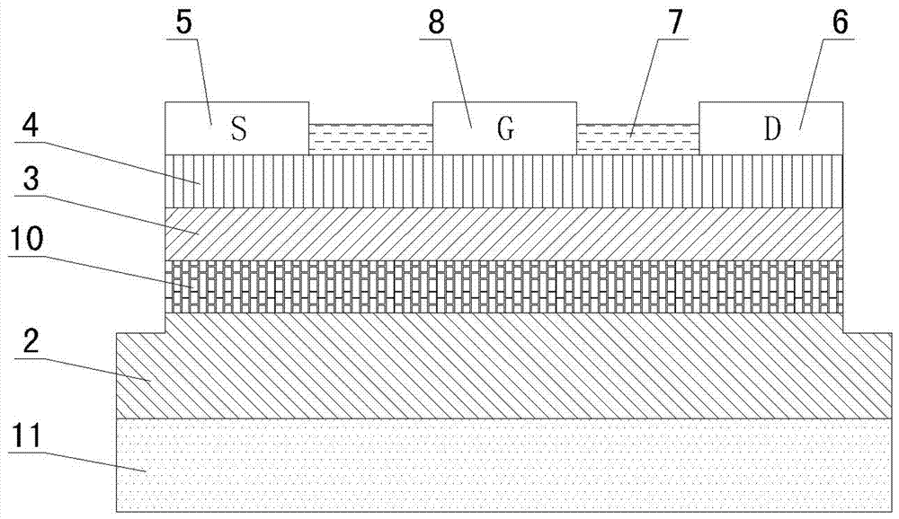
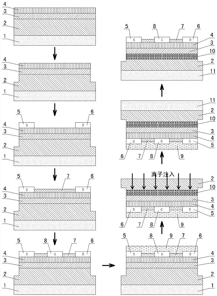
[0053] The embodiment of the present invention provides a method for manufacturing a GaN power device based on ion implantation, which includes the following steps:

[0054] Step 1), using metal organic chemical vapor deposition equipment to sequentially grow GaN buffer layer, GaN channel layer and AlGaN barrier layer on the silicon substrate, the epitaxial growth temperature is between 950°C and 1350°C;

[0055] Step 2) Clean the surface of the AlGaN / GaN sample grown on the silicon substrate. The specific method is: ultrasonic cleaning in acetone and isopropanol solutions for 5 minutes, and then soaking in the mixed solution of sulfuric acid and hydrogen peroxide and pure hydrochloric acid. 10 minutes, and after rinsing in deionized water, blow dry with nitrogen, and use a hot plate to dry the residual moisture on the surface;

[0056] Step 3) Prepare a photoresist mask on the AlGaN barrier layer using a conventional UV lithography process as a pattern for mesa etching in the...

Embodiment 2

[0065] This embodiment differs from Embodiment 1 in that:

[0066] In step 1), a GaN buffer layer, a GaN channel layer and an AlGaN barrier layer are sequentially grown on the SiC substrate;

[0067] Step 5) is to use LPCVD equipment to make SiN x As a passivation layer for GaN power devices, the deposition temperature is 780°C, SiN x The thickness is 300nm;

[0068] In step 8), the silicon carbide substrate is removed by grinding combined with ICP etching.

Embodiment 3

[0070]This embodiment differs from Embodiment 1 in that:

[0071] In step 1), a GaN buffer layer, a GaN channel layer and an AlGaN barrier layer are sequentially grown on the sapphire substrate;

[0072] Step 5) is to use atomic layer deposition equipment (ALD) to make Al 2 o 3 As the passivation layer of the device, the deposition source uses Al-CH 3 And Al-OH, the deposition thickness is 50nm;

[0073] In step 8), the sapphire substrate is removed by laser lift-off; moreover, the ion implantation uses Al ions for implantation isolation and is performed twice, the first implantation is performed with an energy of 135 KeV, and the implantation dose is 5 ×10 14 cm 2 , the second implantation was performed using an energy of 90 KeV with an implantation dose of 3 × 10 14 cm 2 .


PUM


Abstract

The invention discloses a GaN power device based on ion implantation and a manufacturing method thereof. The GaN power device includes a GaN buffering layer, a GaN channel layer and an AiGaN barrier layer which are successively arranged from bottom to top. The A1GaN barrier layer is provided with an active electrode, a gate electrode and a drain electrode thereon, wherein the active electrode and the drain electrode are both ohmic contacts, the gate electrode is a Schottky contact, and all electrodes are covered with a passivation layer therebetween. The passivation layer is connected to the A1Gan barrier layer. The A1Gan barrier layer and the Gan channel layer are heterostructures and the interface between the A1Gan barrier layer and the Gan channel layer forms a 2D electron gas which acts as a transverse working conductive channel of the GaN power device due to polarization effects. An ion isolation region is formed by performing ion implantation on the bottom surface of the GaN buffering layer. The ion isolation region is disposed in the upper part of the GaN buffering layer and is connected to the GaN channel layer, and the GaN buffering layer is provided with an ion isolation region therein and then the bottom surface of the GaN buffering layer is bonded to a high heat conductive substrate. According to the invention, since an ion isolation region is formed by performing ion implantation, the GaN channel and the GaN buffering layer are isolated, such that current leakage is reduced and breakdown voltage is increased.

Description

technical field [0001] The invention relates to the field of semiconductor devices, in particular to a GaN power device based on ion implantation and a manufacturing method thereof. Background technique [0002] As a representative of the third-generation wide-bandgap semiconductor materials, GaN is a new type of semiconductor developed in the past 20 to 30 years after the first generation represented by Si and Ge and the second-generation semiconductor materials represented by GaAs and InP. Material. GaN material has the characteristics of high critical breakdown field strength, large bandgap width, high carrier mobility, high saturated electron drift velocity, and large thermal conductivity. It has incomparable advantages over traditional Si materials and is very suitable for making 300℃), high-power, low-loss power electronic devices can realize the miniaturization, weight reduction and cost reduction of the system, and can make the system more efficient and energy-savin...

Claims


Application Information

Patent Timeline
Patent Type & Authority Applications(China)
IPC IPC(8): H01L21/265H01L21/335H01L29/06H01L29/45H01L29/47H01L29/778
CPCH01L29/0611H01L29/452H01L29/475H01L29/66462H01L29/7783H01L21/265
Inventor 任远陈志涛刘晓燕刘宁炀刘久澄李叶林
Owner GUANGDONG INST OF SEMICON IND TECH
Why Eureka
Try Eureka