

Organic electroluminescent device
a technology of electroluminescence and organic materials, applied in the direction of organic semiconductor devices, thermoelectric devices, organic chemistry, etc., can solve the problems of reducing the film-forming process, reducing the life of conventional charge-generating layers, and reducing the life of driving current, so as to reduce the occurrence of current leakage between pixels, and reduce the occurrence of current leakag
Active Publication Date: 2015-10-22
JOLED INC
View PDF5 Cites 26 Cited by
- Summary
- Abstract
- Description
- Claims
- Application Information
AI Technical Summary
Benefits of technology
The invention relates to a method for making a stacked MPE device that has efficient and low voltage operation, and can suppress current leakage between pixels when forming pixels. This results in a more efficient and effective device for organic light-emitting diodes.
Problems solved by technology
Therefore, there is a problem that, if the driving current is increased in order to increase the initial luminance, the life is shortened with an increase in driving current.
As mentioned above, although various materials are used in a charge-generating layer, there are some problems associated with conventional charge-generating layers.
Specifically, since a high temperature is required when an inorganic substance such as a metal oxide is formed into a film by deposition, the efficiency of film-forming process is lowered, resulting in poor mass productivity.
Further, since a transparent conductor such as an ITO has a high electric conductivity, current leakage between pixels through a charge-generating layer may occur.
This phenomenon becomes a problem especially in the case of a display in which an organic EL device is allowed to emit white color and each of RGB colors is outcoupled through a color filter provided on the device.
In addition, damage to organic layers serving as underlying layers by generated plasma particles is concerned at the time of forming a transparent conductor by sputtering or the like.
However, since HAT itself has high conductivity, as in the case of the above-mentioned transparent conductor, current leakage between pixels through a charge-generating layer may occur.
Method used
View moreImage
Smart ImageViewing Examples

Examples
examples
Blue Organic EL Device
Login to View More PUM
 Abstract
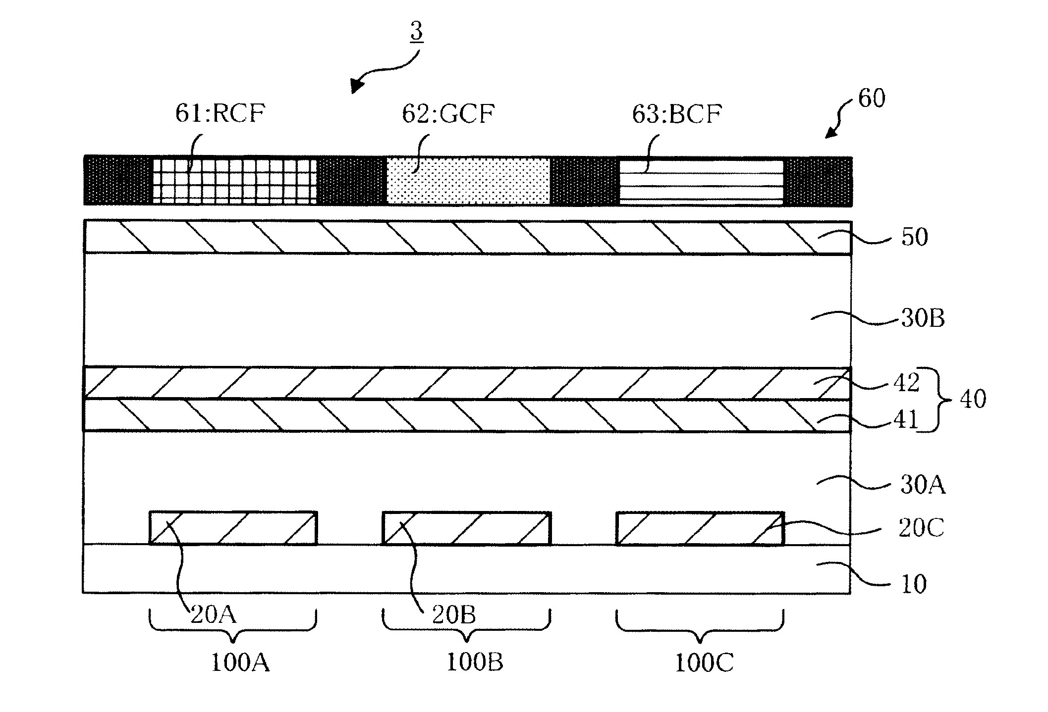
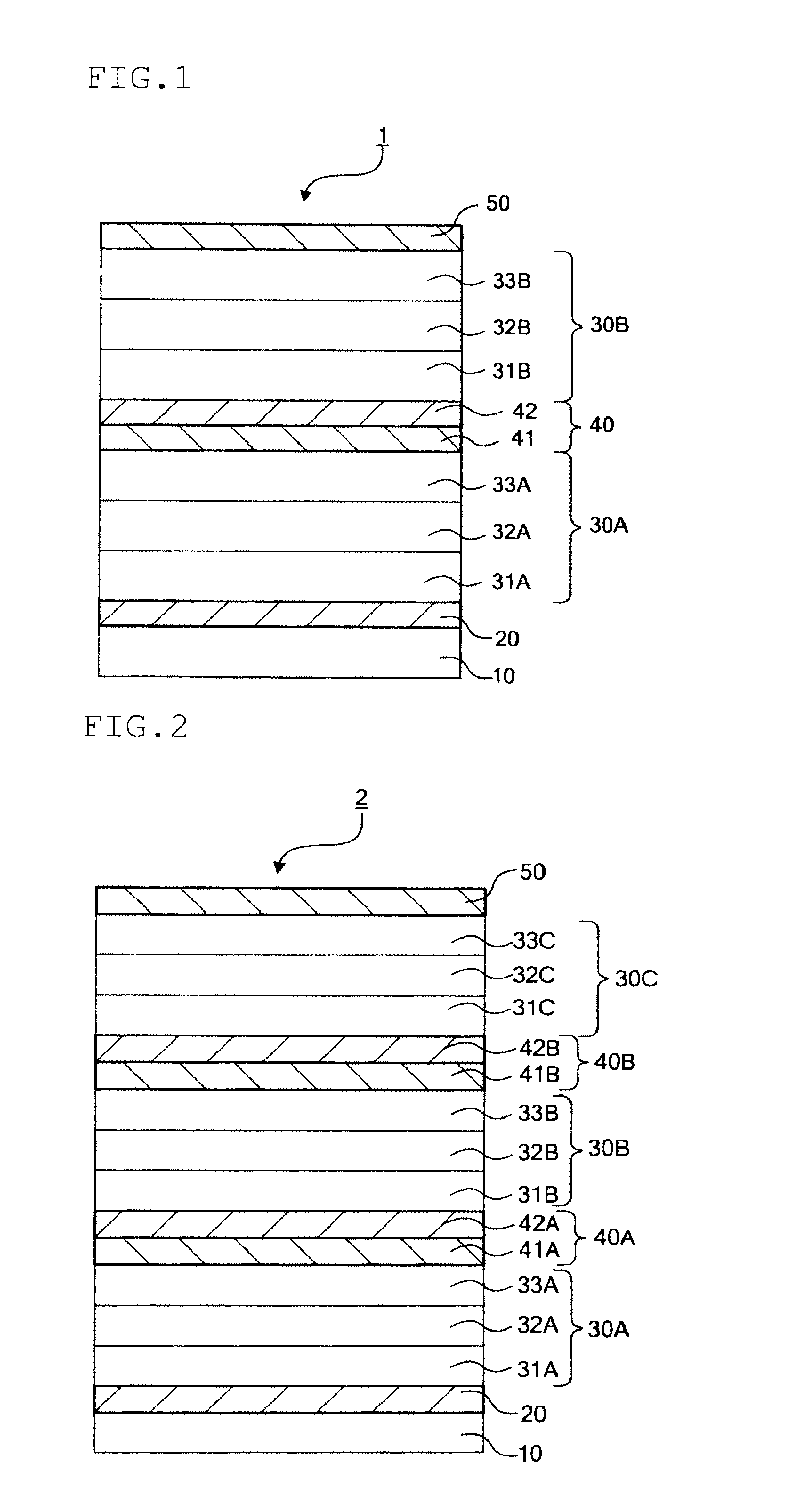
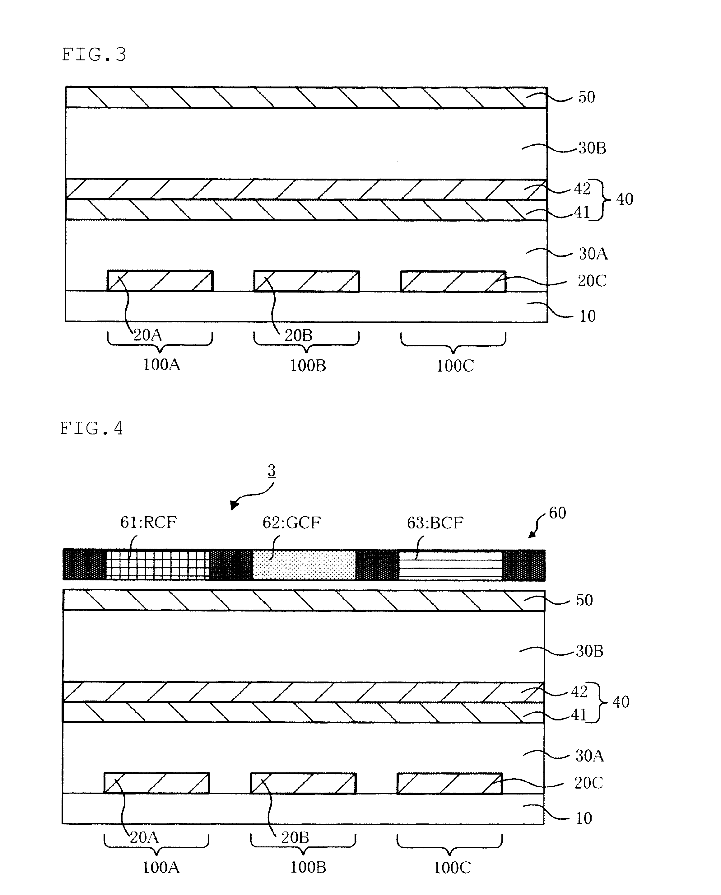
An organic electroluminescence device including: an anode; a cathode; two or more emitting units that are disposed between the anode and the cathode, each unit having an emitting layer; and a charge-generating layer that is disposed between the emitting units, wherein the charge-generating layer includes an N layer nearer to the anode and a P layer nearer to the cathode, and the N layer includes a compound represented by the following formula (I) or (II):
Description
TECHNICAL FIELD[0001]The invention relates to an organic electroluminescence (EL) device. In particular, the invention relates to a stacked multi-photon emission (MPE) device having two or more emitting units.BACKGROUND ART[0002]A common organic EL device comprises an anode that is provided on a substrate and is made of an ITO or the like, an organic layer provided on the anode and a cathode provided on the top of it. The organic layer has a configuration in which a hole-injecting layer, a hole-transporting layer and an emitting layer are stacked in sequence from the side of the anode, for example. In an organic EL device having such a configuration, light that is emitted when electrons injected from a cathode and holes injected from an anode are recombined in an emitting layer is outcoupled from the substrate.[0003]In general, the life of an organic EL device is determined by the amount of injected charges. Therefore, there is a problem that, if the driving current is increased in ...
Claims
Login to View More Application Information
Patent Timeline
 IPC IPC(8): H01L51/00
CPCH01L51/0072H01L51/5056H01L51/0052H01L51/0067H01L51/0054H01L51/0056H01L51/0055H01L51/0073H01L51/0074H01L51/0068H01L51/5206H01L51/5221H01L51/504H01L51/5278H01L2251/533H01L51/5088H01L51/0058C07D487/14C07D471/04C07C255/35C07C255/37C07C255/50C07C255/61C07C261/04C07C255/34C07C255/41C07C2603/40C07C2603/52C07C2603/54H10K59/32H10K59/38H10K59/17H10K85/611H10K85/615H10K85/6572H10K50/19H10K85/622H10K85/623H10K85/624H10K85/626H10K85/654H10K85/655H10K85/6574H10K85/6576H10K50/13H10K50/15H10K50/17H10K50/81H10K50/82H10K2102/3035
InventorKAMBE, EMIKONAKAMURA, MASATOFUNAHASHI, MASAKAZUYAMAMOTO, HIROSHIMIZUTANI, SAYAKA
OwnerJOLED INC