Nitride semiconductor, nitride semiconductor crystal growth method, and nitride semiconductor light emitting element

a nitride semiconductor and crystal growth technology, applied in the direction of crystal growth process, polycrystalline material growth, chemically reactive gas, etc., can solve the problem of high dislocation density, insufficient dislocation density of ingan in blue-color light-emitting regions normally used as quantum well layers of gan-based leds, and unavoidable gan crystal epitaxial growth on sapphire substrates. , to achieve the effect of improving the crystallinity of the n

Active Publication Date: 2010-09-30
MITSUBISHI CHEM CORP
View PDF8 Cites 53 Cited by
  • Summary
  • Abstract
  • Description
  • Claims
  • Application Information

AI Technical Summary

Benefits of technology

[0050]According to the present invention, an inactive gas which does not have etching effect on nitrides is selected as a gas which constitutes the main flow during the period from the heating step in a relatively high temperature region before the nitride semiconductor layers are grown to the completion of growth of the nitride semiconductor layers, thereby controlling the atmosphere to which the principal nitride plane of the base is exposed. Besides, no Si source is provided when the growth of the nitride semiconductor layers is initiated. Consequently, nitrogen atoms are less liable to leave from near the surface of the nitride on the epitaxial base. This prevents defects from being introduced into the epitaxial films and enables epitaxial growth characterized by surface morphology of excellent flatness.
[0051]Also, according to the present invention, the thickness of the (first) nitride semiconductor layer (not intentionally doped with Si) is optimized, where the (first) nitride semiconductor layer is the initial layer of crystal growth of the nitride semiconductor. This makes it possible to improve crystallinity of the nitride semiconductor epitaxially grown on the (first) nitride semiconductor layer.
[0052]Thus, as a result of these effects, the present invention readily provides a high-quality nitride semiconductor using a nonpolar plane as a growth substrate, the nitride semiconductor being characterized by sufficiently low dislocation density and good surface morphology and optical characteristics as well as high luminous efficiency when used as a light-emitting element.

Problems solved by technology

Since sapphire and GaN differ greatly in lattice constant, a considerable dislocation on the order of 109 / cm2 is unavoidable for a GaN crystal epitaxially grown on a sapphire substrate.
Moreover, light-emitting efficiencies of InGaN in blue-color light-emitting regions normally used as quantum well layers of GaN-based LEDs are insufficiently sensitive to dislocation density.
However, when gallium nitride-based semiconductor crystals are viewed as a material for devices used under conditions of high carrier density, high dislocation density such as described above considerably deteriorates device characteristics.
For example, high dislocation density remarkably reduces the life of devices such as high-power LEDs or lasers.
However, surface flatness and optical characteristics of a nitride semiconductor crystal obtained through epitaxial growth on a substrate whose principal plane is the polar plane cannot be said to be quite sufficient, and growth conditions require further examination.
Besides, a problem resulting inevitably from the use of the polar plane as a growth substrate has also been recognized.
However, epitaxial growth on nonpolar planes of hexagonal III-V nitride crystals, i.e., on the a-plane, r-plane, and m-plane, is considered to be difficult, and in particular, high-quality, stacked, hexagonal III-V nitride semiconductor structures cannot be obtained on the m-plane at present.
However, it is stated that the resulting GaN layer was “slate-like.” There were severe surface irregularities and a single-crystal GaN layer was not available.

Method used


Image

  • Nitride semiconductor, nitride semiconductor crystal growth method, and nitride semiconductor light emitting element
  • Nitride semiconductor, nitride semiconductor crystal growth method, and nitride semiconductor light emitting element
  • Nitride semiconductor, nitride semiconductor crystal growth method, and nitride semiconductor light emitting element

Examples


example 1

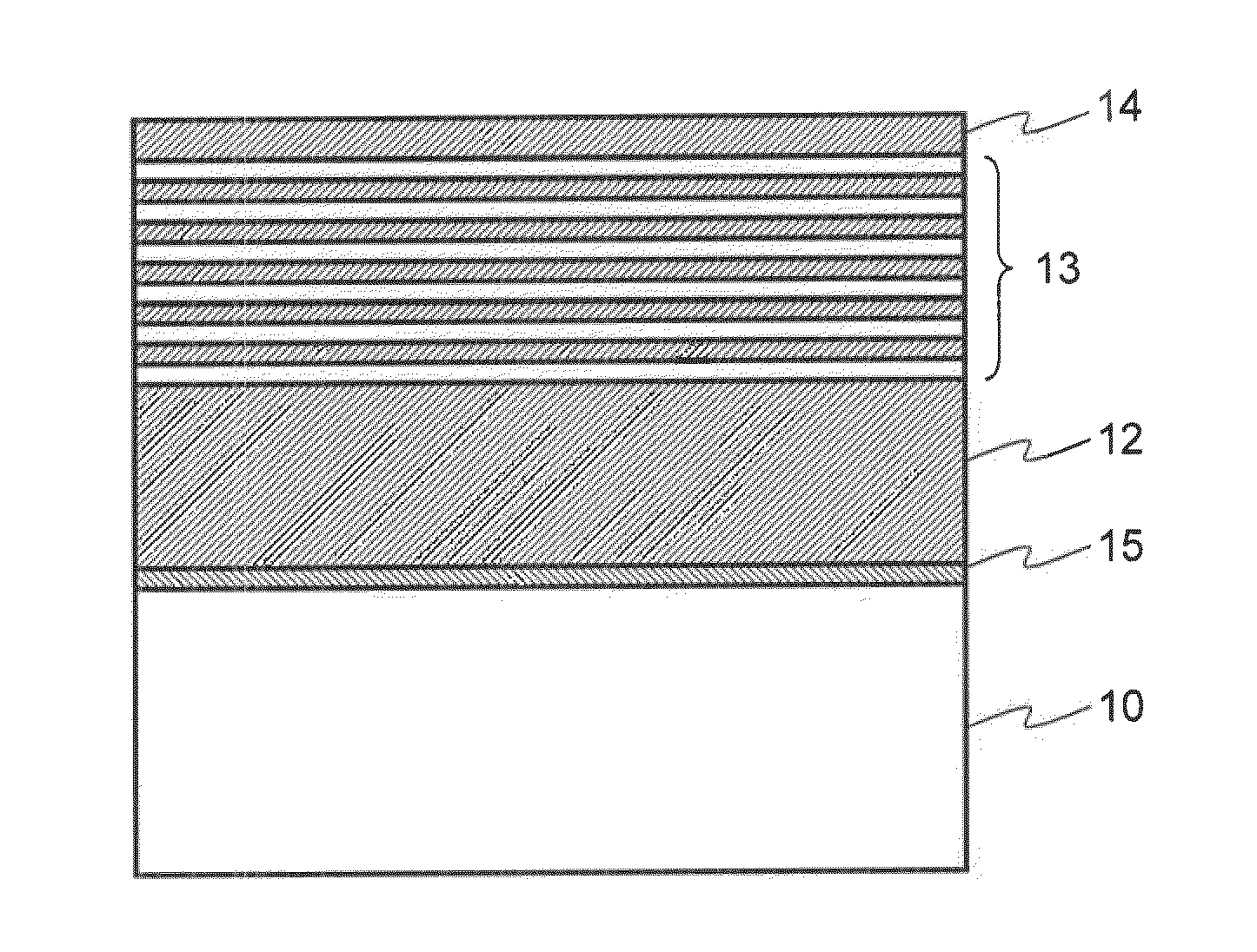
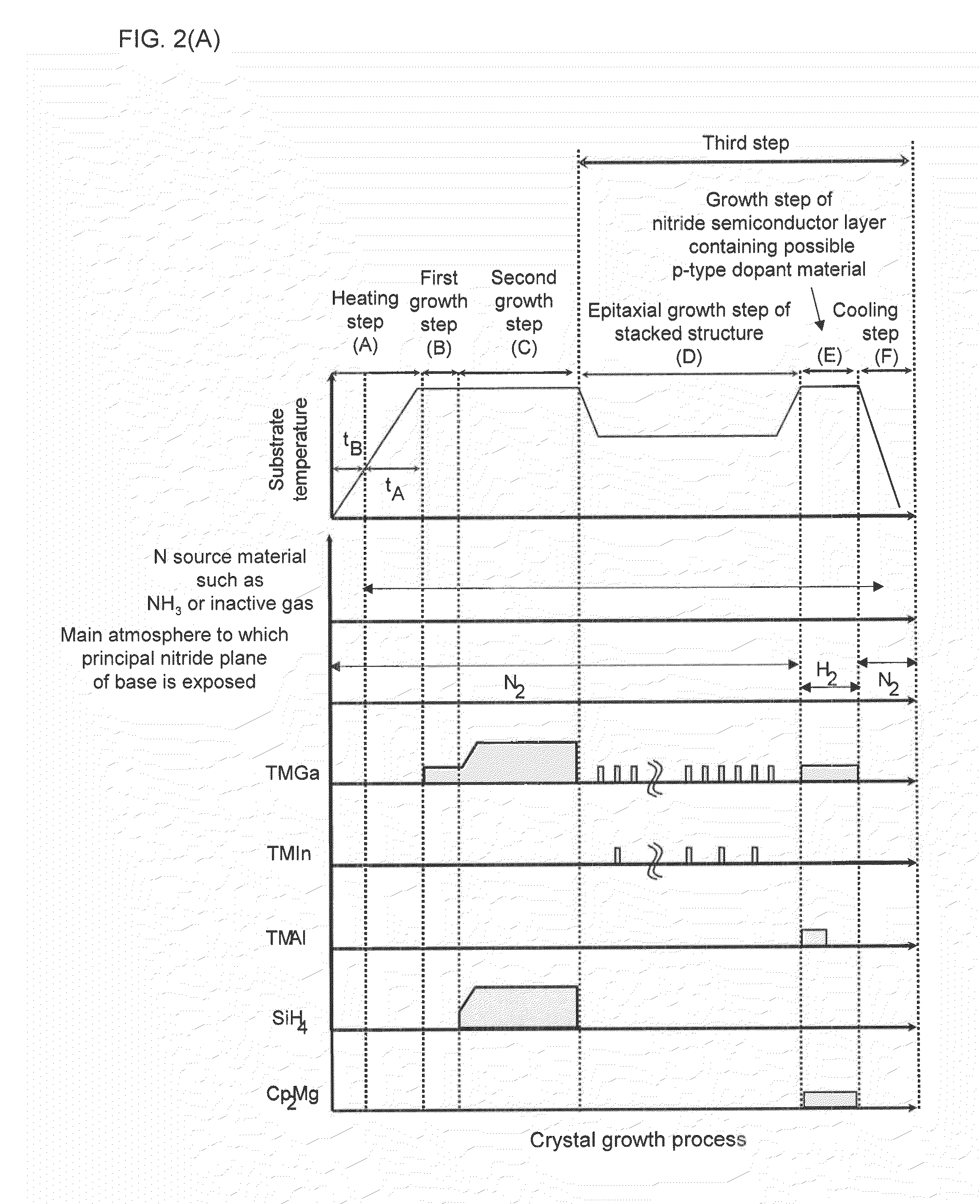
[0226]In the present example, a stack of gallium nitride-based semiconductor thin films was grown by the MOCVD process and a near ultraviolet LED was fabricated. A series of crystal growth processes for that has already been outlined with reference to FIG. 2(A). Also, a layer structure after growth is schematically shown in FIG. 3(A).

[0227]The base used was a (1-100) m-plane oriented freestanding GaN substrate. The substrate measured 4.1 mm in the c-axis direction and 15 mm in the a-axis direction. Regarding electrical characteristics, the substrate was n-type and carrier density was 6.6×1017 cm−3. As a result of X-ray diffraction, the full-width at half maximum of a (10-12) reflection rocking curve was 34.2 arcsec., OFF angle in the c(+) direction was 0.25 degrees, and OFF angle in the A direction was 0.03 degrees. Also, the dislocation density was 5.0×106 cm−2.

[0228]The m-plane freestanding GaN substrate was placed on a tray (susceptor) in a horizontal quartz reactor which normall...

example 2

[0244]In the present example, a stack of gallium nitride-based semiconductor thin films was grown by the MOCVD process and a near ultraviolet LED was fabricated. A series of crystal growth processes for that has already been outlined with reference to FIG. 2(A). Also, a layer structure after growth is schematically shown in FIG. 3(A).

[0245]The base used was a (1-100) m-plane oriented freestanding GaN substrate. The substrate measured 4.2 mm in the c-axis direction and 15 mm in the a-axis direction. Regarding electrical characteristics, the substrate was n-type and carrier density was 6.7×1017 cm−3. As a result of X-ray diffraction, the full-width at half maximum of a (10-12) reflection rocking curve was 32.8 arcsec., OFF angle in the c(+) direction was 0.29 degrees, and OFF angle in the a direction was 0.05 degrees. Also, the dislocation density was 5.4×106 cm−2. The m-plane freestanding GaN substrate was placed on a tray (susceptor) in a horizontal quartz reactor which normally ope...

example 3

[0253]In the present example, a stack of gallium nitride-based semiconductor thin films was grown by the MOCVD process and a near ultraviolet LED was fabricated. A series of crystal growth processes for that has already been outlined with reference to FIG. 2(A). Also, a layer structure after growth is schematically shown in FIG. 3(A).

[0254]The base used was a (1-100) m-plane oriented freestanding GaN substrate. The substrate measured 4.0 mm in the c-axis direction and 15 mm in the a-axis direction. Regarding electrical characteristics, the substrate was n-type and carrier density was 6.4×1017 cm−3. As a result of X-ray diffraction, the full-width at half maximum of a (10-12) reflection rocking curve was 36.7 arcsec., OFF angle in the c(+) direction was 3.0 degrees, and OFF angle in the a direction was 0.3 degrees. Also, the dislocation density was 5.1×106 cm−2. The m-plane freestanding GaN substrate was placed on a tray (susceptor) in a horizontal quartz reactor which normally opera...


PUM

PropertyMeasurementUnit
areaaaaaaaaaaa
surface roughness Raaaaaaaaaaa
temperatureaaaaaaaaaa

Abstract

During the growth of a nitride semiconductor crystal on a nonpolar face nitride substrate, such as an m-face, the gas that constitutes the main flow in the process of heating up to a relatively high temperature range, before growth of the nitride semiconductor layer, (the atmosphere to which the main nitride face of the substrate is exposed) and the gas that constitutes the main flow until growth of first and second nitride semiconductor layers is completed (the atmosphere to which the main nitride face of the substrate is exposed) are primarily those that will not have an etching effect on the nitride, while no Si source is supplied at the beginning of growth of the nitride semiconductor layer. Therefore, nitrogen atoms are not desorbed from near the nitride surface of the epitaxial substrate, thus suppressing the introduction of defects into the epitaxial film. This also makes epitaxial growth possible with a surface morphology of excellent flatness.

Description

TECHNICAL FIELD [0001]The present invention relates to a nitride semiconductor crystal growth technique, and more particularly, to a crystal growth technique for obtaining a high-quality nitride semiconductor with excellent surface conditions and optical characteristics.BACKGROUND ART [0002]A blue-color light-emitting element or ultraviolet light-emitting element can be used as a white light source if combined with an appropriate wavelength conversion material. Active studies have been conducted on applications of such white light sources to backlights for liquid crystal displays and the like, light-emitting diode illumination, automotive lighting, general lighting to replace fluorescent lighting, and so on. Some of the studies have already been put to practical use. Today, such blue-color light-emitting elements and ultraviolet light-emitting elements are produced mainly by growing a thin film of gallium nitride-based semiconductor crystal using a technique such as a metal-organic ...

Claims


Application Information

Patent Timeline
Patent Type & Authority Applications(United States)
IPC IPC(8): H01L33/30H01L29/20C30B23/02H01L33/00H01L33/16
CPCC30B25/02C30B29/403H01L21/0237H01L21/02433H01L21/02458H01L33/16H01L21/0262H01L21/02658H01L33/007H01L33/0075H01L21/0254
Inventor HORIE, HIDEYOSHIKURIHARA, KAORI
Owner MITSUBISHI CHEM CORP
Why Eureka
Try Eureka