

Semiconductor substrate and its production method, semiconductor device comprising the same and its production method
a semiconductor substrate and production method technology, applied in the direction of individual semiconductor device testing, semiconductor/solid-state device testing/measurement, instruments, etc., can solve the problems of productivity and quality, disadvantages and disadvantages, and it is extremely difficult to etch or polish the silicon substrate to 1 .mu.m or less with good accuracy and uniformity
- Summary
- Abstract
- Description
- Claims
- Application Information
AI Technical Summary
Benefits of technology
Problems solved by technology
Method used
Image

Examples
embodiment 1
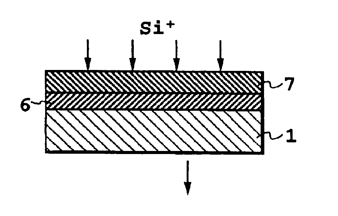
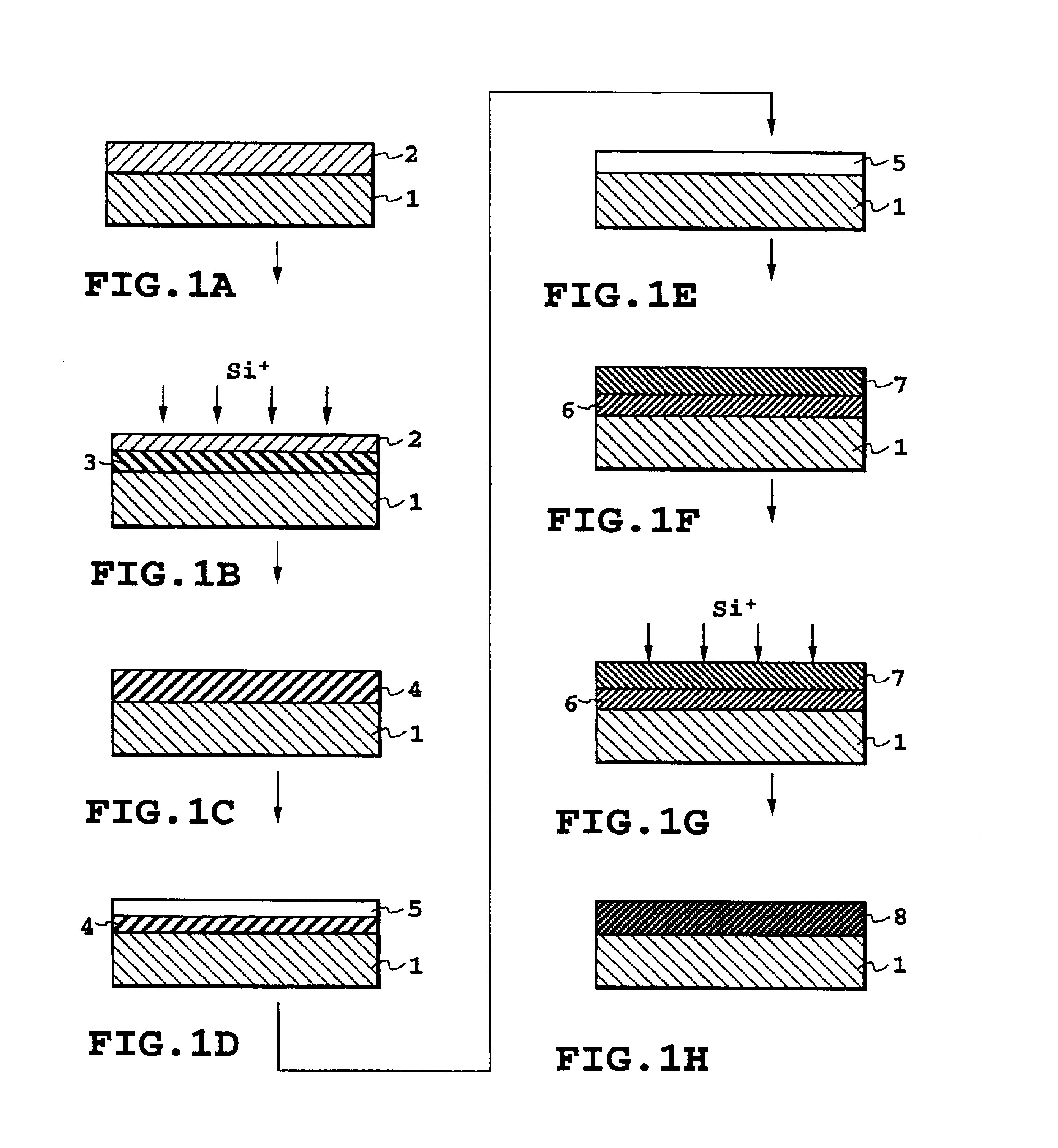
On a R-plane sapphire substrate, by a LPCVD method using monosilane (SiH.sub.4) gas as a source material, a first silicon layer was grown to a thickness of 280 nm at a growing temperature of 950.degree. C. This first silicon layer was implanted with silicon ion of energy 190 keV in an amount of 1.times.10.sup.16 / cm.sup.2 as a first ion implantation while maintaining the substrate temperature at 0.degree. C. to make the interface side with sapphire amorphous. After that, as a first heat treatment, in a nitrogen gas atmosphere, heat treatment at temperature 550.degree. C. for 30 minutes, then at temperature 900.degree. C. for 60 minutes was performed to recrystallize the silicon layer. Next, the resulting product was introduced in an oxidation furnace, and subjected to water vapor oxidation at 1000.degree. C. for 60 minutes. Then, after immersing in BHF to remove oxide film, it was again water vapor oxidized at 900.degree. C. for 50 minutes. This oxide film was removed, and the thick...
embodiment 2
A SOS substrate was produced using the same procedure as in Embodiment 1 except that when forming the second silicon layer, the silicon layer was stacked at a growing temperature of 750.degree. C. by the UHV-CVD method monosilane as a source material.
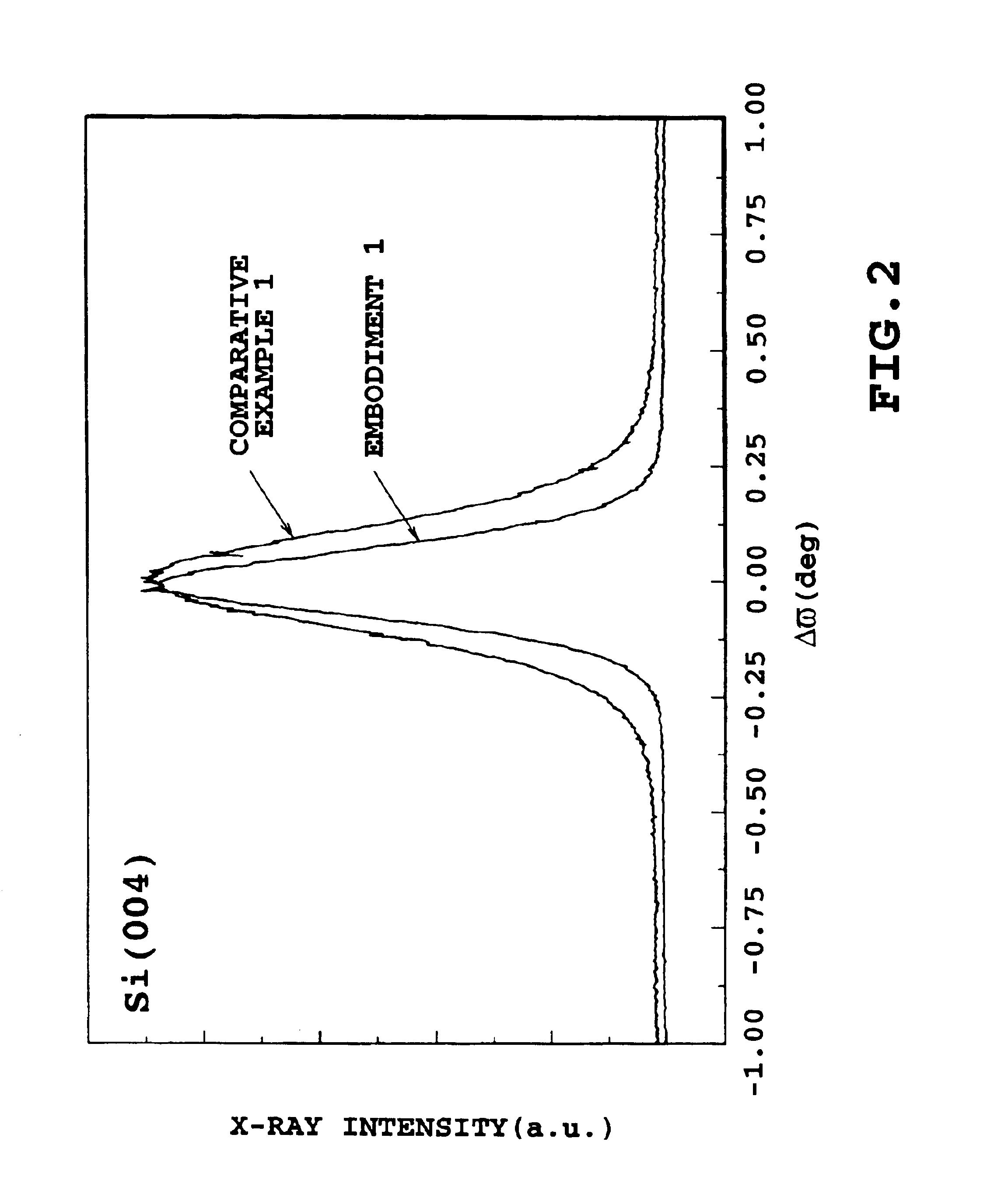
When the resulting substrate was measured for crystalline defect density and rocking curve full width at half maximum by the same method as in Embodiment 1, the crystal defect density was 2.5.times.10.sup.6 / cm.sup.2, the (004) plane full width at half maximum was 0.167 degree, and the (040) full width at half maximum was 0.120 degree. The (004) plane full width at half maximum was constant in the depth direction, and crystallinity was uniform in the depth direction of the silicon layer. Further, the surface roughness (Rrms) of the silicon layer was 1.0 nm.
When, using this substrate, a n-type MOSFET was produced and evaluated for transistor characteristics as in Embodiment 1. The threshold voltage was 0.7 V, variation of drain current d...
embodiment 3
A SOS substrate was produced using the same procedure as in Embodiment 1 except that after recrystallization by the first heat treatment, when the silicon layer was oxidized, oxidation was performed at 1000.degree. C. for 10 hours instead of water vapor oxidation at 1000.degree. C. for 60 minutes.
When the resulting substrate was measured for crystalline defect density and rocking curve full width at half maximum as in the same method as Embodiment 1, the crystalline defect density was 6.8.times.10.sup.6 / cm.sup.2, the (004) full width at half maximum 0.205 degree and the (040) full width at half maximum 0.140 degree. The (040) full width at half maximum was constant in the depth direction, and the crystallinity was uniform in the depth direction of the silicon layer. Further, the surf ace roughness (Rrms) of the silicon layer was 1.5 nm.
When, using this substrate, a n-type MOSFET was produced as in Embodiment 1, and evaluated for transistor characteristics. The threshold voltage was...
PUM
 Abstract
Description
Claims
Application Information