Semiconductor device, semiconductor device production method, and substrate for the semiconductor device

a semiconductor device and semiconductor technology, applied in the direction of semiconductor devices, basic electric elements, electrical appliances, etc., can solve the problems of poor planarity of gan compound crystal portions grown in the openings of stripe pattern masks, inability to eliminate height differences, and failure to achieve excellent planarity, etc., to achieve excellent crystallinity, excellent surface planarity, and excellent light-emitting efficiency

Inactive Publication Date: 2006-04-20
ROHM CO LTD
View PDF1 Cites 70 Cited by
  • Summary
  • Abstract
  • Description
  • Claims
  • Application Information

AI Technical Summary

Benefits of technology

[0041] This method makes it possible to produce a light emitting diode structure. In the light emitting diode structure, carriers are injected into the active layer from the gallium nitride compound semiconductor layer of the first conductivity and the gallium nitride compound semiconductor layer of the second conductivity, whereby positive holes and electrons are recombined in the active layer to provide light emission. Thus, a gallium nitride compound sem

Problems solved by technology

However, it was impossible to eliminate height differences occurring at junctions of the GaN compound crystal portions grown from the mask openings, failing to achieve excellent planarity.
Where the substrate having the offset

Method used


Image

  • Semiconductor device, semiconductor device production method, and substrate for the semiconductor device
  • Semiconductor device, semiconductor device production method, and substrate for the semiconductor device
  • Semiconductor device, semiconductor device production method, and substrate for the semiconductor device

Examples


first embodiment

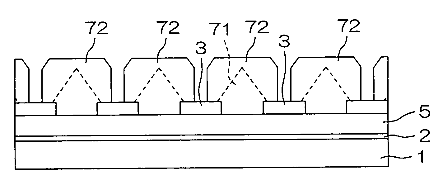
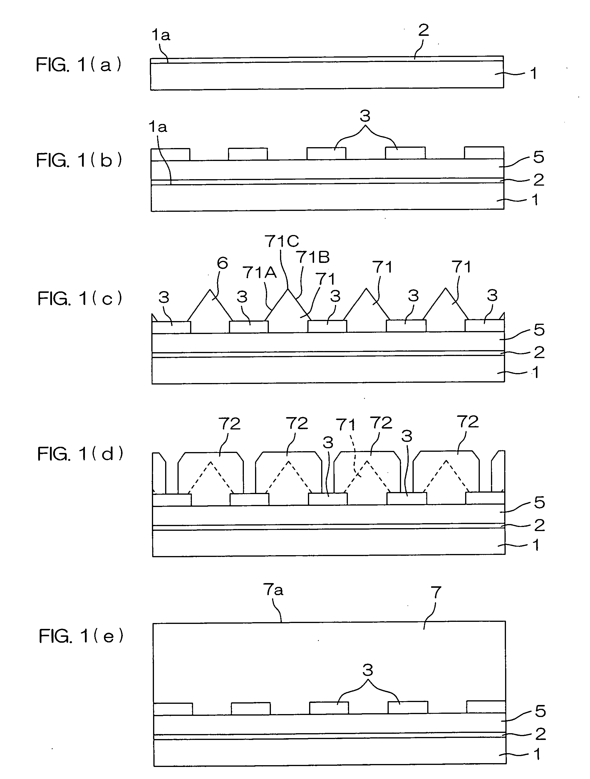
[0063] FIGS. 1(a) to 1(e) are sectional views illustrating steps of a semiconductor device production method according to the present invention. A substrate 1 composed of sapphire, crystalline silicon carbide or crystalline aluminum nitride is prepared. The substrate 1 has a major surface la offset from a C-plane by a predetermined offset angle. A buffer layer 2 is formed on the major surface 1a of the substrate 1 (see FIG. 1(a)). The buffer layer 2 is composed of a Group III nitride compound represented by Inx1Aly1Ga1-x1-y1N (0≦x1≦1, 0≦y1≦1, 0≦x1+y1≦1). The formation of the buffer layer 2 may be achieved, for example, by an epitaxial growth method such as an MOCVD (metal-organics chemical vapor deposition) method. The buffer layer 2 has a thickness of about 200 Å, for example.

[0064] A GaN compound semiconductor film 5 (hereinafter referred to as “underlying GaN film 5”) is formed as an underlying film on the buffer layer 2 to provide crystal nuclei for crystal growth (see FIG. 1(b)...

second embodiment

[0083] FIGS. 4(a) to 4(e) are sectional views illustrating steps of a semiconductor device production method according to the present invention. In FIGS. 4(a) to 4(e), parts corresponding to those shown in FIGS. 1(a) to 1(e) will be denoted by the same reference characters as in FIGS. 1(a) to 1(e).

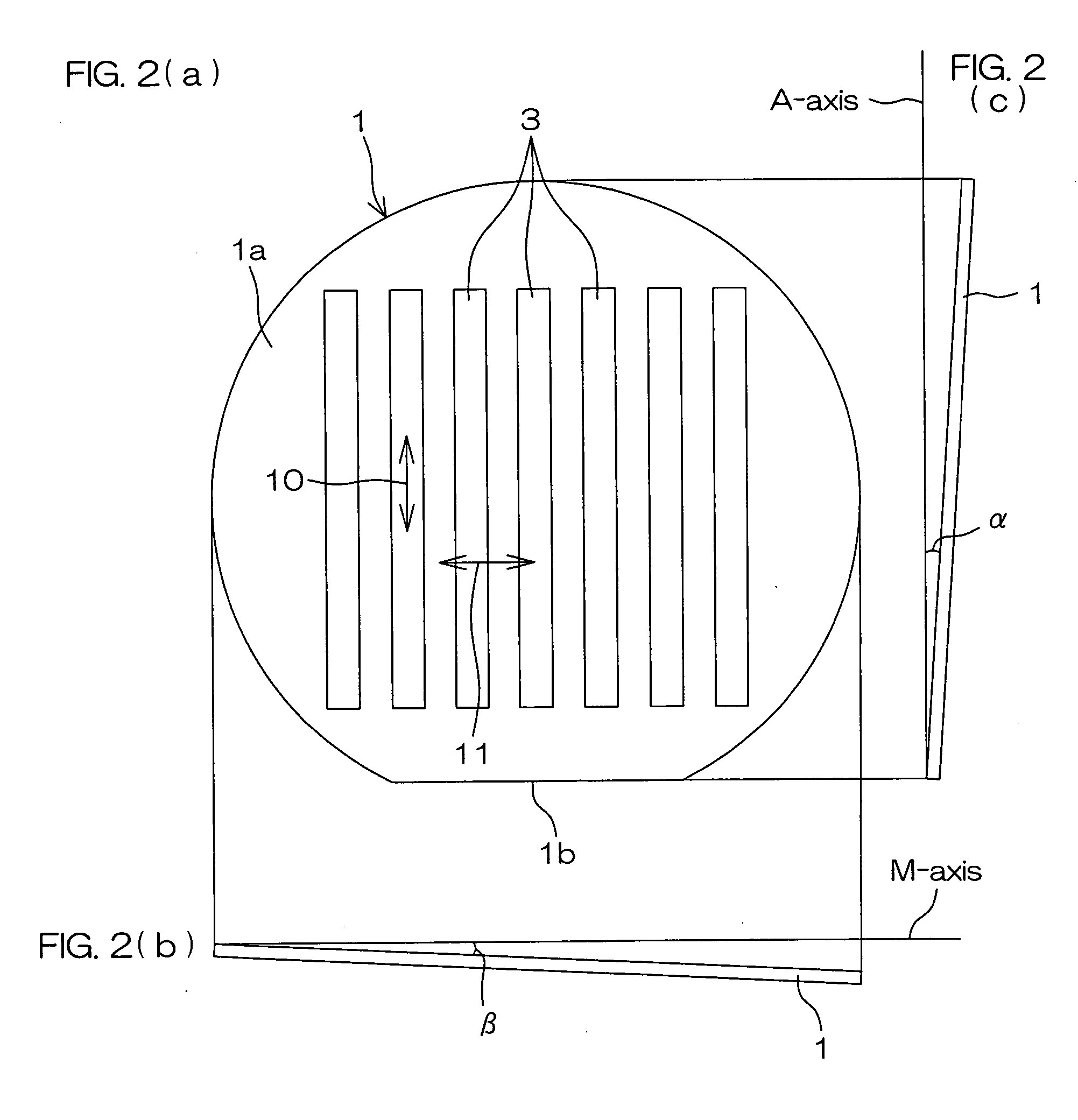
[0084] In this embodiment, a buffer layer 2 and an underlying GaN film 5 are formed on a substrate 1, and then undulations are formed in a stripe configuration in a surface of the underlying GaN film 5. More specifically, the formation of the undulations is achieved, for example, by forming a plurality of etching masks 12 in an equidistant stripe pattern (in a linear parallel stripe pattern in this embodiment) on the surface of the underlying GaN film 5 by photolithography (FIG. 4(a)) and forming a plurality of linear recesses (grooves) 13 in an equidistant stripe pattern in the surface of the underlying GaN film 5 by etching with the use of the etching masks 12 (FIG. 4(b) ). Portions of t...

third embodiment

[0093] FIGS. 8(a) to 8(e) are sectional views illustrating steps of a semiconductor device production method according to the present invention. In FIGS. 8(a) to 8(e), parts corresponding to those shown in FIGS. 1(a) to l(e) will be denoted by the same reference characters as in FIGS. 1(a) to 1(e).

[0094] In this embodiment, undulations are formed in a linear stripe pattern in a surface of a substrate 1 by etching or dicing (FIG. 8(a)). That is, a plurality of linear recesses 21 (grooves) are formed in an equidistant stripe pattern in the surface of the substrate 1, so that linear projections 22 are each defined between two adjacent linear recesses 21. Thus, the stripe pattern (linear parallel stripe pattern in this embodiment) is formed as having the plurality of linear recesses 21 and the plurality of linear projections 22. The linear recesses 21 each have a depth of about 3 μm, for example.

[0095] In this state, a buffer layer 2 (e.g., having a thickness of about 200 Å) is formed ...


PUM


Abstract

A semiconductor device production method includes the steps of: forming a linear gallium nitride stripe pattern on a major surface of a substrate, the major surface of the substrate being offset from a predetermined crystal plane by offset angles of 0.1 degree to 0.5 degrees respectively defined with respect to a first crystal axis and a second crystal axis parallel to the predetermined crystal plane, the linear gallium nitride stripe pattern extending along the first crystal axis; and growing a gallium nitride compound semiconductor crystal along the predetermined crystal plane by selective lateral epitaxial growth to form a gallium nitride compound semiconductor layer on the major surface of the substrate formed with the gallium nitride stripe pattern. The first crystal axis and the second crystal axis may be perpendicular to each other. The substrate may be a sapphire substrate, a silicon carbide substrate, an aluminum nitride substrate or a gallium nitride substrate. In this case, the predetermined crystal plane is preferably a C-plane.

Description

BACKGROUND OF THE INVENTION [0001] 1. Field of the Invention [0002] The present invention relates to a semiconductor device based on a gallium nitride compound semiconductor, a production method for the semiconductor device, and a substrate for the semiconductor device. [0003] 2. Description of Related Art [0004] Gallium nitride (GaN) compound semiconductors are represented by a general formula InxAlyGa1-x-yN (0≦x<1, 0≦y<1, 0≦x+y<1). Since the gallium nitride compound semiconductors have different band gaps within the range of 1.95 eV to 6 eV depending on their compositions, the gallium nitride compound semiconductors are attractive as materials for light emitting devices having a wide range of wavelengths from the ultraviolet to the infrared. [0005] In a typical production process for a semiconductor light emitting device based on such a GaN compound semiconductor, a light emitting diode structure is produced by forming a GaN compound crystal layer on a sapphire monocrysta...

Claims


Application Information

Patent Timeline
IPC IPC(8): H01L21/20H01L33/12H01L33/16H01L33/32H01L33/34H01L33/48
CPCH01L21/0237H01L21/0242H01L21/02433H01L21/02458H01L21/0254H01L21/02642H01L21/02647H01L33/007
Inventor KOHDA, SHINICHI
Owner ROHM CO LTD
Why Eureka
Try Eureka