

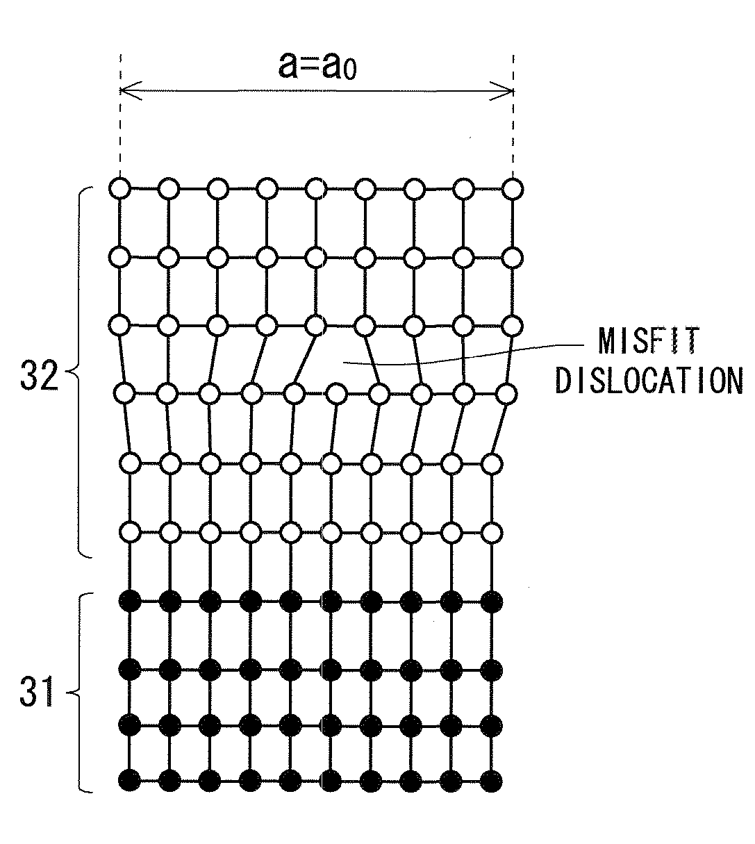
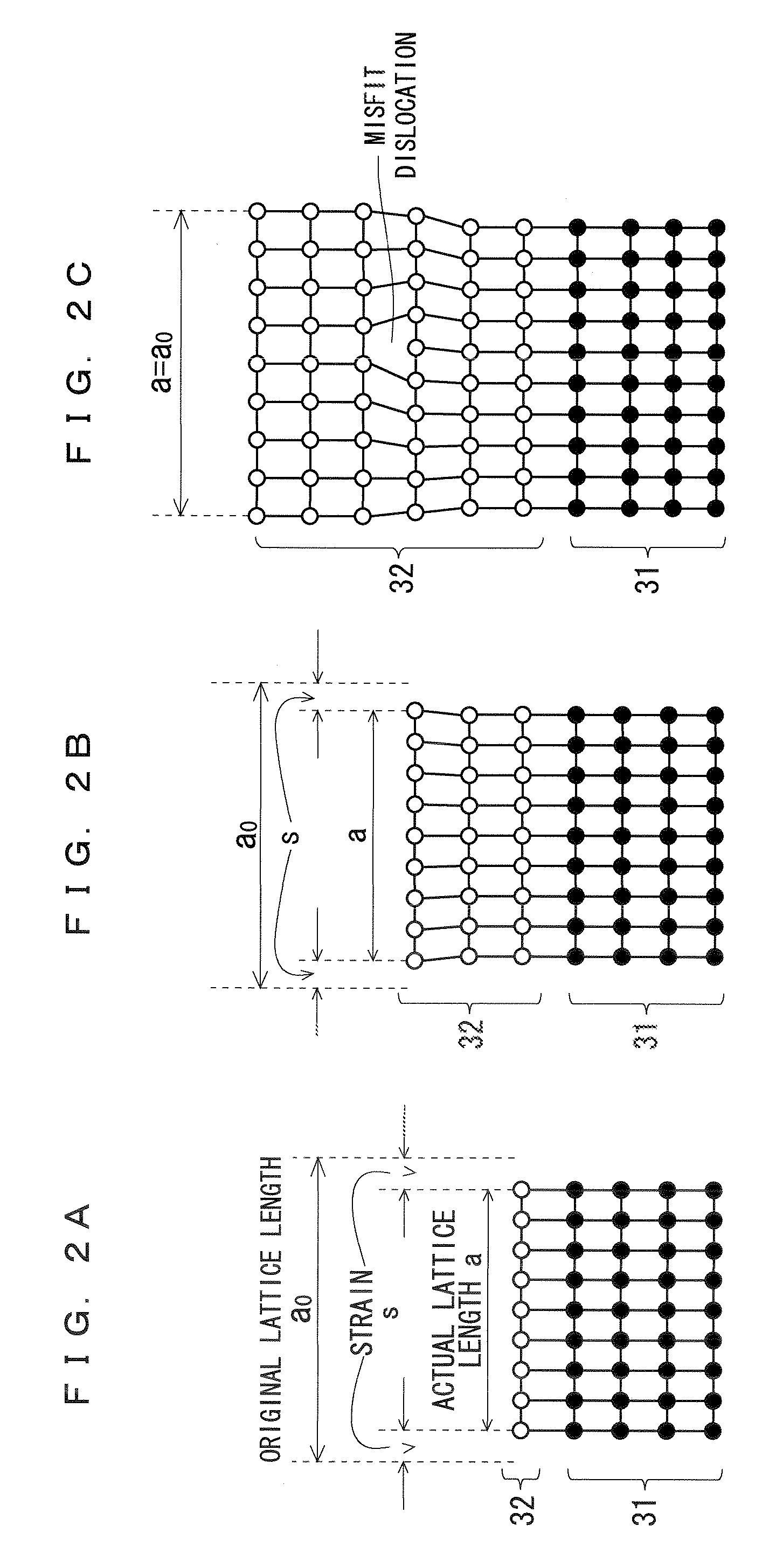
Epitaxial substrate and method for manufacturing epitaxial substrate
a technology of epitaxial substrate and nitride, which is applied in the direction of crystal growth process, polycrystalline material growth, chemically reactive gas growth, etc., can solve the problems of reducing the yield of nitride films, affecting the formation of good nitride films, and difficult to form a good nitride film on silicon substrates. , to achieve the effect of enhancing the compressive strain introduced by the superlattice layer group, reducing
- Summary
- Abstract
- Description
- Claims
- Application Information
AI Technical Summary
Benefits of technology
Problems solved by technology
Method used
Image

Examples
examples
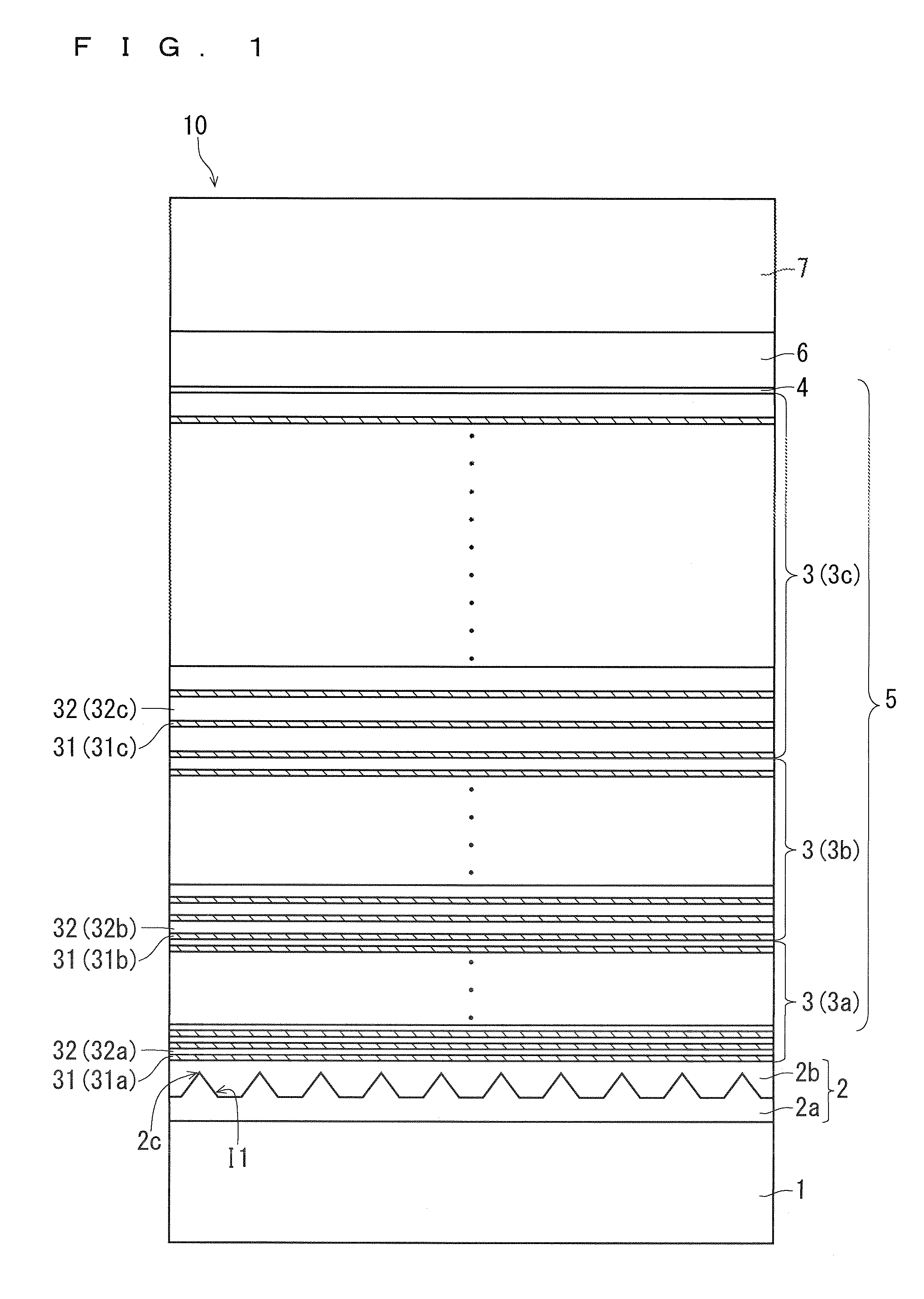
[0110]Epitaxial substrates 10 according to five examples (examples 1 to 5) different from one another in terms of the configuration of the superlattice layer group 5, and an epitaxial substrate 100 according to a comparative example including only a single superlattice layer instead of the superlattice layer group 5, were prepared. FIG. 4 is a schematic cross-sectional view showing an outline configuration of the epitaxial substrate 100. In the epitaxial substrate 100, a first unit layer 8a and a second unit layer 8b form a pair layer, and one superlattice layer 8 is formed. FIG. 5 is a diagram showing a list of a specific preparation condition, a total film thickness, the amount of warping, and the presence or absence of occurrence of cracking, for each of the epitaxial substrates according to the respective examples and the comparative example.
[0111]Until the formation of the second base layer 2b, the same procedure was performed in both the examples and the comparative examples. ...
PUM
| Property | Measurement | Unit |
|---|---|---|
| thickness | aaaaa | aaaaa |
| thickness | aaaaa | aaaaa |
| thickness | aaaaa | aaaaa |
Abstract
Description
Claims
Application Information