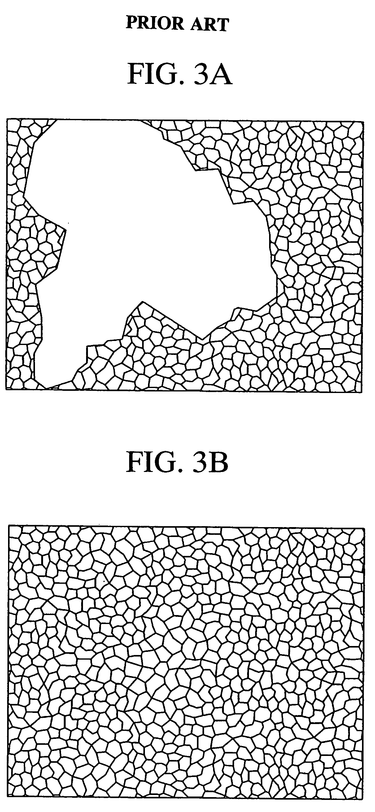
[0011] The conductive layers may use a rolled material comprising 20 ppm or more of each of Cu, Fe and Si. The conductive layers may be rolled with a draft of at least 15%. In such cases, abnormal growth of the Al crystals can be suppressed, enabling a reduction in the variation of the crystal grain diameter.
[0012] The surface area of the crystal with the maximum crystal grain diameter preferably accounts for no more than 15% of the surface area of the insulating ceramic substrate. In such cases, the effect of the present invention in preventing
anisotropy of the mechanical characteristics of the conductive layers is particularly strong.
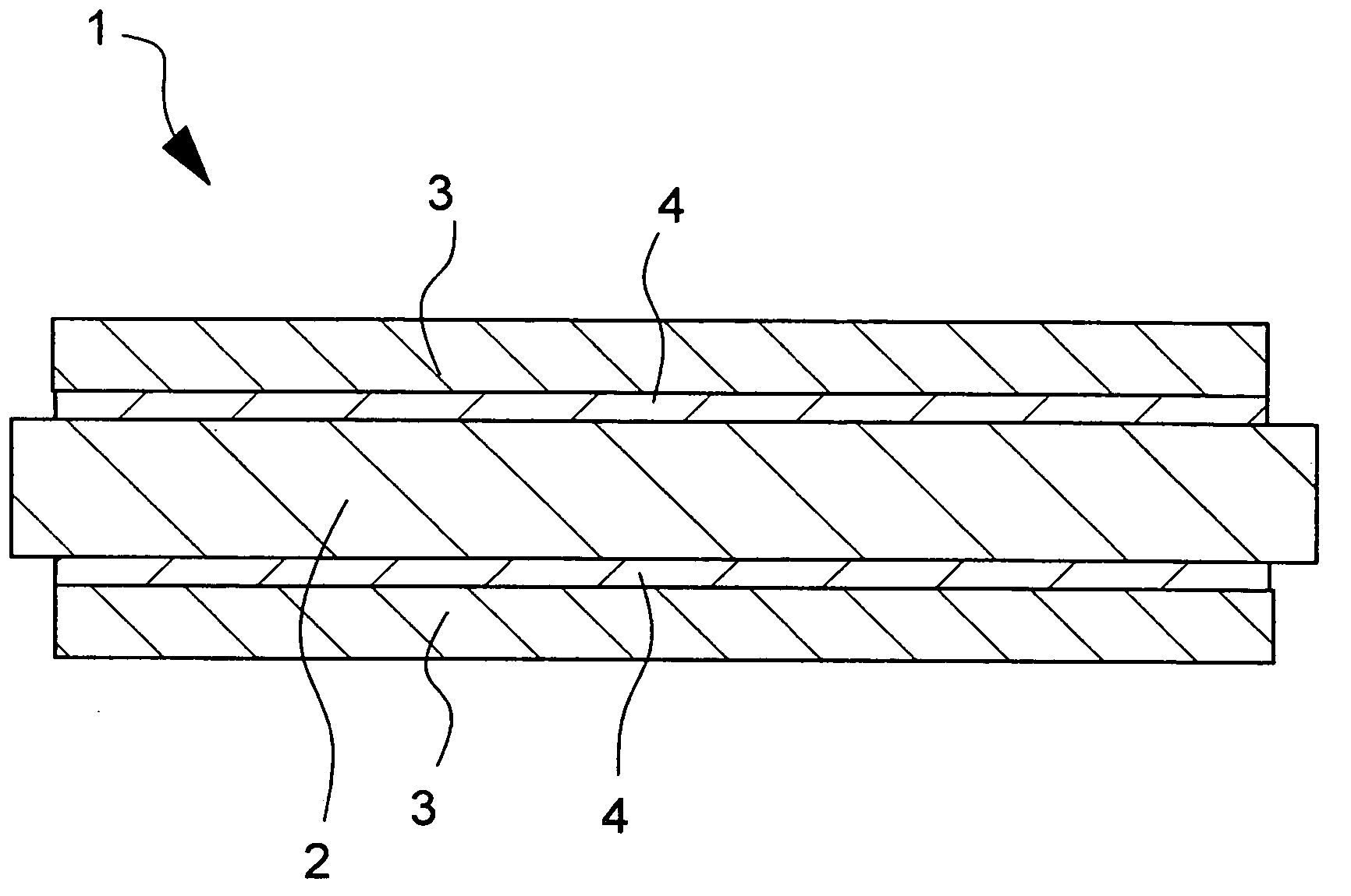
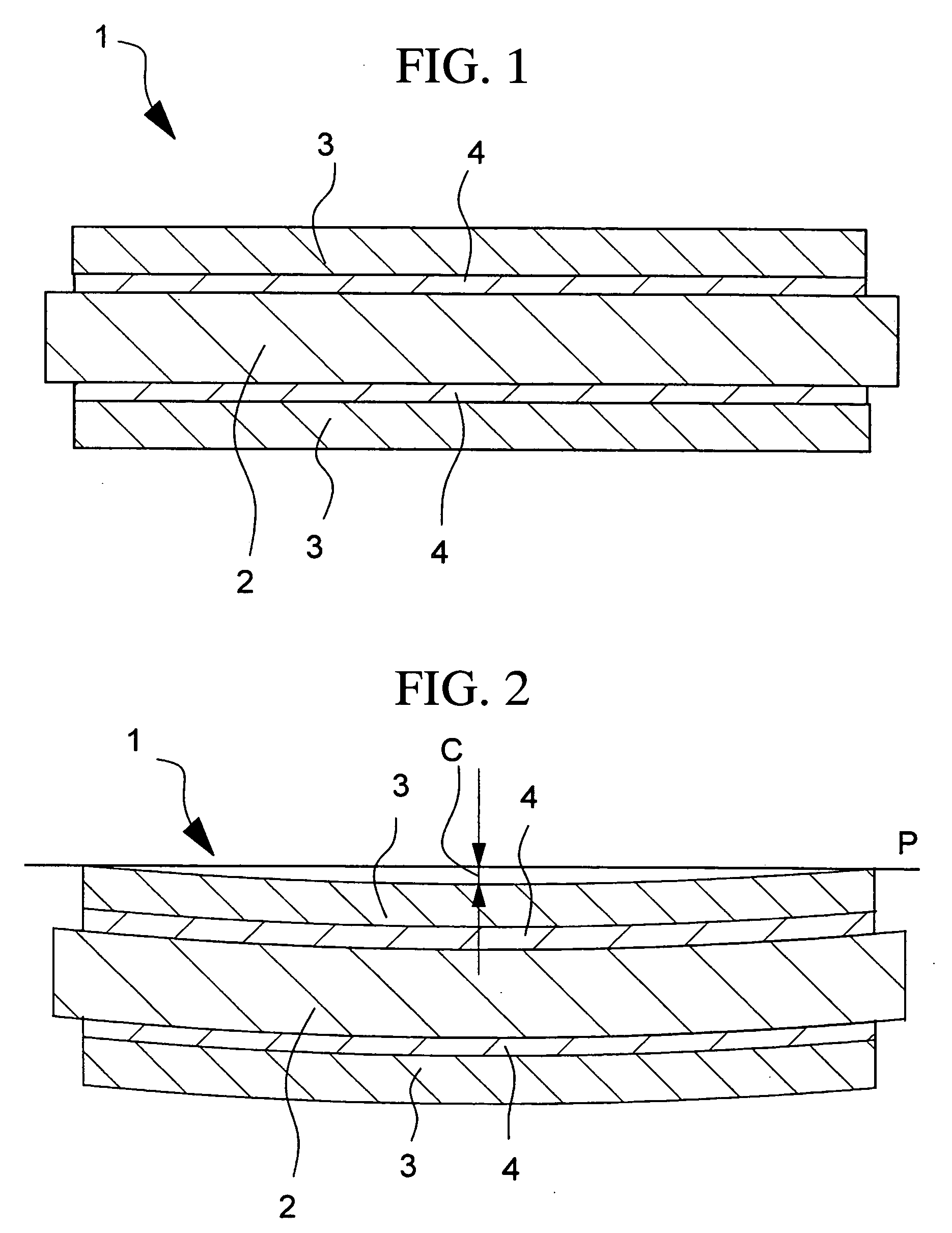
[0013] The insulating ceramic substrate may be formed from at least one of Al2O3, AlN and Si3N4. The conductive layers may be bonded to the insulating ceramic substrate using a brazing material. The brazing material may be one or more materials selected from a group consisting of Al—Si based materials, Al—Ge based materials, Al—Mn based materials, Al—Cu based materials, Al—Mg based materials, Al—Si—Mg based materials, Al—Cu—Mn based materials, and Al—Cu—Mg—Mn based materials. In such cases, the bonding between the conductive layers and the insulating ceramic substrate is favorable.
[0016] The above production method may comprise an additional step for producing the conductive layer by
heat treating a plate material comprising at least 99.98% by
mass of aluminum, and then conducting rolling with a draft of at least 15%. By ensuring a draft of at least 15% from the final heat treatment, the 0.2% proof stress value of the conductive layer can be set at no more than approximately 35 N / mm2, and the Al material
work hardening coefficient can be set at no more than approximately 0.18. As a result, the effect of the present invention in preventing
cracking of the ceramic substrate on
exposure to repeated temperature variations can be further strengthened. For example, if a −40° C. to 125° C. temperature cycle test is conducted, then the number of cycles before
cracking develops in the substrate can be increased. A temperature cycle test is a test in which a
temperature treatment, in which a
single cycle involves, for example, holding the circuit board at −40° C. for 30 minutes and then at 125° C. for 30 minutes in a
thermal shock tester, is carried out repeatedly.
[0017] According to the present invention, because the average crystal grain diameter of the conductive layer is kept within a range from 0.5 mm to 5 mm, and the standard deviation σ of the crystal grain diameter is no more than 2 mm,
anisotropy is unlikely to develop in the mechanical characteristics of the conductive layer, enabling a reduction in the occurrence of warping of the circuit board. Furthermore, because the conductive layer comprises at least 99.98% by
mass of aluminum, the stress alleviating capabilities of the layer are good, and cracking of the ceramic substrate is unlikely even when exposed to temperature variation. Accordingly, the present invention enables not only a reduction in the warping of the circuit board, but also enables prevention of other problems such as cracking of the ceramic substrate on
exposure to temperature variation.
[0019] The average crystal grain diameter of the conductive layer is even more preferably within a range from 0.8 mm to 1.5 mm, and the standard deviation a of the crystal grain diameter is even more preferably 1 mm or smaller. In such cases, problems such as cracking of the ceramic substrate on
exposure to temperature variation can be even more reliably prevented.

