Exposure apparatus and exposure method, and device manufacturing method

a technology of exposure apparatus and exposure method, which is applied in the direction of microlithography exposure apparatus, printers, instruments, etc., can solve the problems of small quantity of pollutants that are very likely to stick to the surface of optical elements, the exposure light energy on the wafer (a substrate subject to exposure) becomes unstable, and the transmission in the optical system decreases, so as to achieve stable exposure intensity and accurately formed

Inactive Publication Date: 2005-01-11
NIKON CORP
View PDF14 Cites 152 Cited by
  • Summary
  • Abstract
  • Description
  • Claims
  • Application Information

AI Technical Summary

Benefits of technology

[0064]In addition, because by performing exposure using an exposure apparatus according to this invention in a lithography process, exposure is performed with stable exposure intensity, patterns can be accurately formed on a substrate. Therefore, it is possible to manufacture highly-integrated micro devices with high yield and improved productivity. Furthermore, because by using an exposure method according to this invention in a lithography process, exposure is performed with stable exposure intensity, patterns can be accurately formed on a substrate. Accordingly, it is possible to manufacture highly-integrated micro devices with high yield and improved productivity. Therefore, according to another aspect of this invention, there are provided a device manufacturing method using an exposure apparatus or exposure method according to this invention.

Problems solved by technology

However, because an exposure apparatus used in mass-production of integrated circuits such as LSI's needs to expose about 80 wafers per hour to exposure light, there is a large possibility of absorbent gas from the outside getting into the optical path of exposure light from the projection optical system to the wafer upon the frequent replacement of wafers.
If absorbent gas gets into the optical paths of exposure light due to those factors, absorption rate and thus transmission fluctuate to some extent depending on the concentration of the absorbent gas, and exposure light energy on the wafer (a substrate subject to exposure) becomes unstable.
Furthermore, if there is water or organic pollutants in the optical paths, a small quantity of such pollutants are very likely to stick to the surfaces of optical elements.
Because the pollutants greatly absorb vacuum ultraviolet light (exposure light), transmission in the optical systems decreases due to the small quantity of pollutants sticking to the surfaces of the optical elements.
Therefore, pollutants in the optical paths cause variation of exposure light transmission.

Method used


Image

  • Exposure apparatus and exposure method, and device manufacturing method
  • Exposure apparatus and exposure method, and device manufacturing method
  • Exposure apparatus and exposure method, and device manufacturing method

Examples


first embodiment

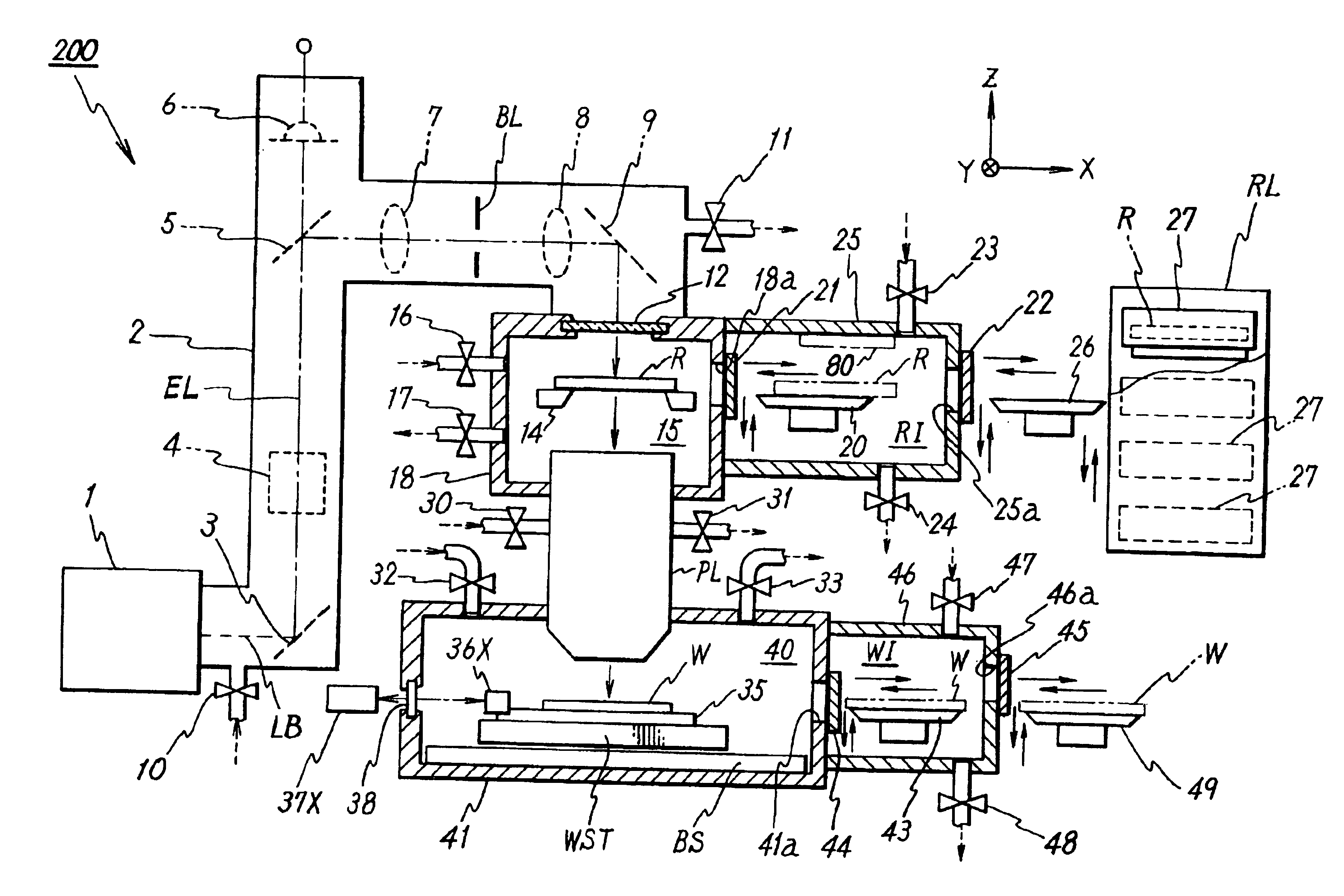
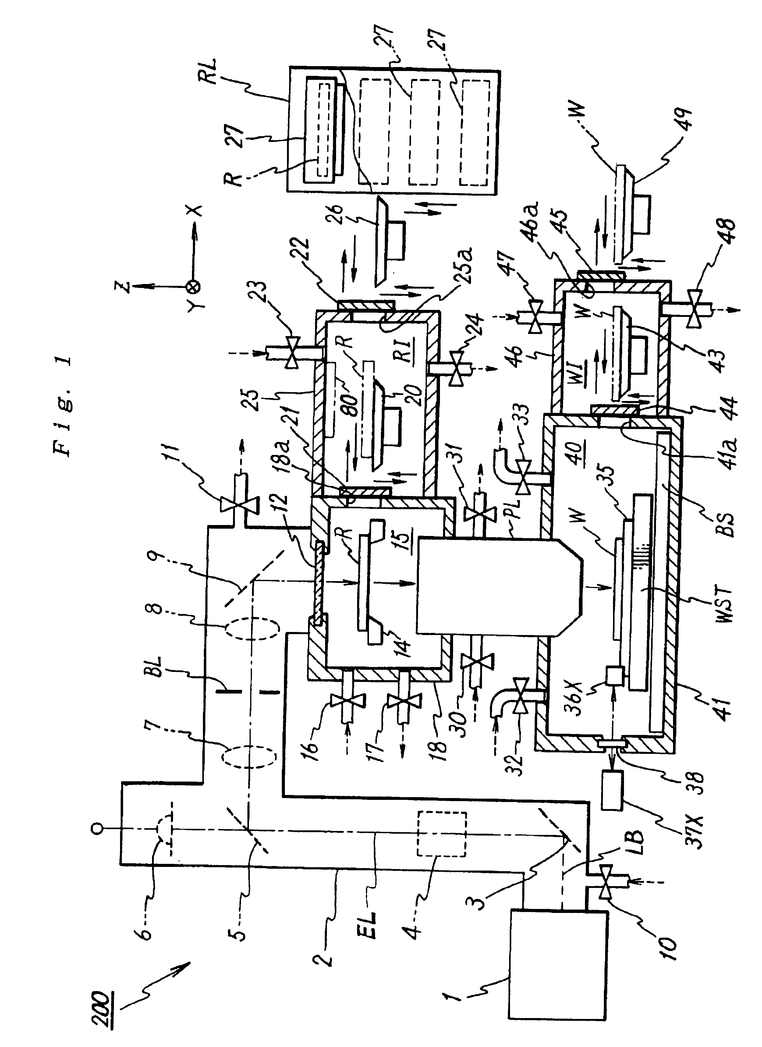
[0065]FIG. 1 is a schematic view showing a partial section through an exposure apparatus ;

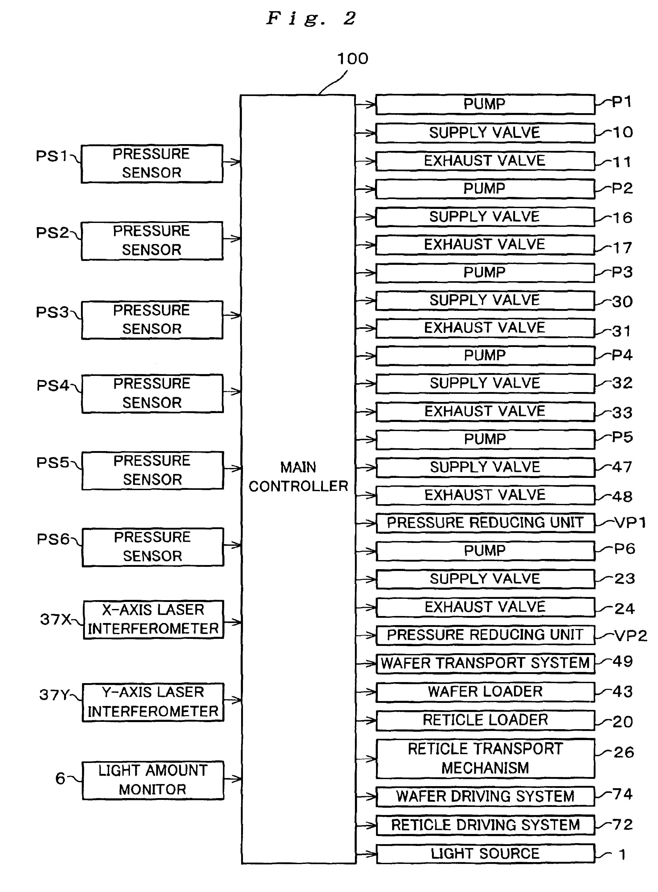
[0066]FIG. 2 is a block diagram showing main components of the control system of the apparatus in FIG. 1;

[0067]FIG. 3 is a schematic view showing the gas piping system of the apparatus in FIG. 1;

[0068]FIG. 4A is a plan view of reticle R with the pattern surface facing up, and FIG. 4B is a cross-sectional view taken along line B-B in FIG. 4A;

[0069]FIG. 5 is a view showing a modified example of a wafer stage;

[0070]FIG. 6 is a plan view showing an example of the arrangement in which two wafer-gas-replacement rooms are arranged;

second embodiment

[0071]FIG. 7 is a cross-sectional view through a reticle-gas-replacement room ;

[0072]FIG. 8A is a schematic, oblique view of an exemplary reticle library for which a circulation mechanism of low-absorbent gas is provided, and FIG. 8B is an enlarged, cross-sectional view of the joint portion of the reticle library and a supply mechanism 54 in FIG. 4A;

third embodiment

[0073]FIG. 9 is a cross-sectional view through a reserve room ;

[0074]FIG. 10 is a flow chart for explaining a device manufacturing method according to this invention; and

[0075]FIG. 11 is a flow chart showing a process of step 204 of FIG. 10;


PUM

PropertyMeasurementUnit
wavelengthaaaaaaaaaa
timeaaaaaaaaaa
spends timeaaaaaaaaaa

Abstract

After a mask is carried into a reserve room for temporarily storing before carrying into a mask room filled with specific gas that has an impurity concentration lower than a first concentration (e.g. 1 ppb) and that has a characteristic of absorbing little exposure light, gas-replacement mechanisms replace gas in the reserve room with specific gas having an oxygen concentration not lower than the first concentration. Therefore, when subsequently carrying the mask into the mask room, impurities from the outside (including absorbent gas) can be substantially prevented from getting into the optical path inside the mask room. When replacing a wafer, gas in a reserve room is also replaced in the same way as the above.

Description

TECHNICAL FIELD[0002]The present invention relates to an exposure apparatus and exposure method, and a device manufacturing method and more particularly to an exposure apparatus and exposure method used in forming fine patterns on electronic devices such as semiconductor integrated circuits and liquid crystal displays, and a device manufacturing method using the exposure apparatus and exposure method.BACKGROUND ART[0003]In forming fine patterns on electronic devices such as semiconductor integrated circuits and liquid crystal displays, a method has been used which transfers a pattern, having a size about 4 to 5 times the size of an actual pattern on the wafer, on a photo-mask or a reticle (both to be referred to as a “reticle” hereinafter) onto a substrate subject to exposure such as a wafer, reducing the pattern by using a reduction-projection exposure apparatus such as a stepper.[0004]In projection exposure apparatuses for transferring a pattern, exposure apparatuses of a newer ge...

Claims


Application Information

Patent Timeline
Patent Type & Authority Patents(United States)
IPC IPC(8): G03F7/20
CPCG03F7/70741G03F7/70933G03F7/70866G03F7/7075
Inventor SHIRAISHI, NAOMASA
Owner NIKON CORP
Why Eureka
Try Eureka