Exposure apparatus and exposure method, and device manufacturing method

a technology of exposure apparatus and exposure method, which is applied in the direction of photomechanical treatment, printing, instruments, etc., can solve the problems of large amount of measurement and time, the prior art method of measuring and adjusting aberrations based on limited information hardly meets the demand for further improvement of exposure accuracy, and the effect of accurate formation

Inactive Publication Date: 2006-12-21
NIKON CORP
View PDF33 Cites 59 Cited by
  • Summary
  • Abstract
  • Description
  • Claims
  • Application Information

AI Technical Summary

Benefits of technology

[0033] In addition, in a lithography process, by performing exposure using the exposure apparatus of the present invention, a pattern can accurately be formed on an object, which makes it possible to manufacture highly integrated microdevices with high yield. Therefore, according to another aspect of the present invention, there is provided a device manufacturing method in which the exposure apparatus of the present invention is used. In addition, in a lithography process, by performing exposure using the exposure method of the present invention, a pattern can accurately be formed on a photosensitive object. Therefore, further according to another aspect of the present invention, there is provided a device manufacturing method in which the exposure method of the present invention is used (i.e. a device manufacturing method including a process in which a pattern is transferred onto an object using the exposure method).

Problems solved by technology

However, because of the demand for further improved exposure accuracy corresponding to increasingly high integration in these years, measuring only the lower-order aberrations according to the prior art method and, based on the measurement result, adjusting the optical properties of the projection optical system does not yield a desired result.
Therefore, the prior art method of measuring and adjusting aberrations based on the limited information hardly meet the demand for further improved exposure accuracy.
In this case, although reticle patterns having intrinsic frequency components that are missing in the information need to be measured, it takes an enormous amount of measurement and time, so that it is not practical.
Furthermore, when an aberration is large, the linearity of the resist image to the corresponding aerial image of the pattern is lost, so that accurate measurement of the aberration is difficult.
It is because a projection optical system satisfying the specification determined obviously cannot achieve exposure accuracy demanded at present and in the future.
However, the above method of making a projection optical system needs the two steps of correcting lower-order aberrations and correcting higher-order aberrations and also computation for ray-tracing that even super-computer will take several days to perform.
For example, when coma is large, the image of a pattern is not resolved, so that accurate data of distortion, astigmatism and spherical aberration cannot be obtained.
The fact that the order of measuring the aberrations to be adjusted is specified means that the selection of the lenses used is restricted.

Method used


Image

  • Exposure apparatus and exposure method, and device manufacturing method
  • Exposure apparatus and exposure method, and device manufacturing method
  • Exposure apparatus and exposure method, and device manufacturing method

Examples


Embodiment Construction

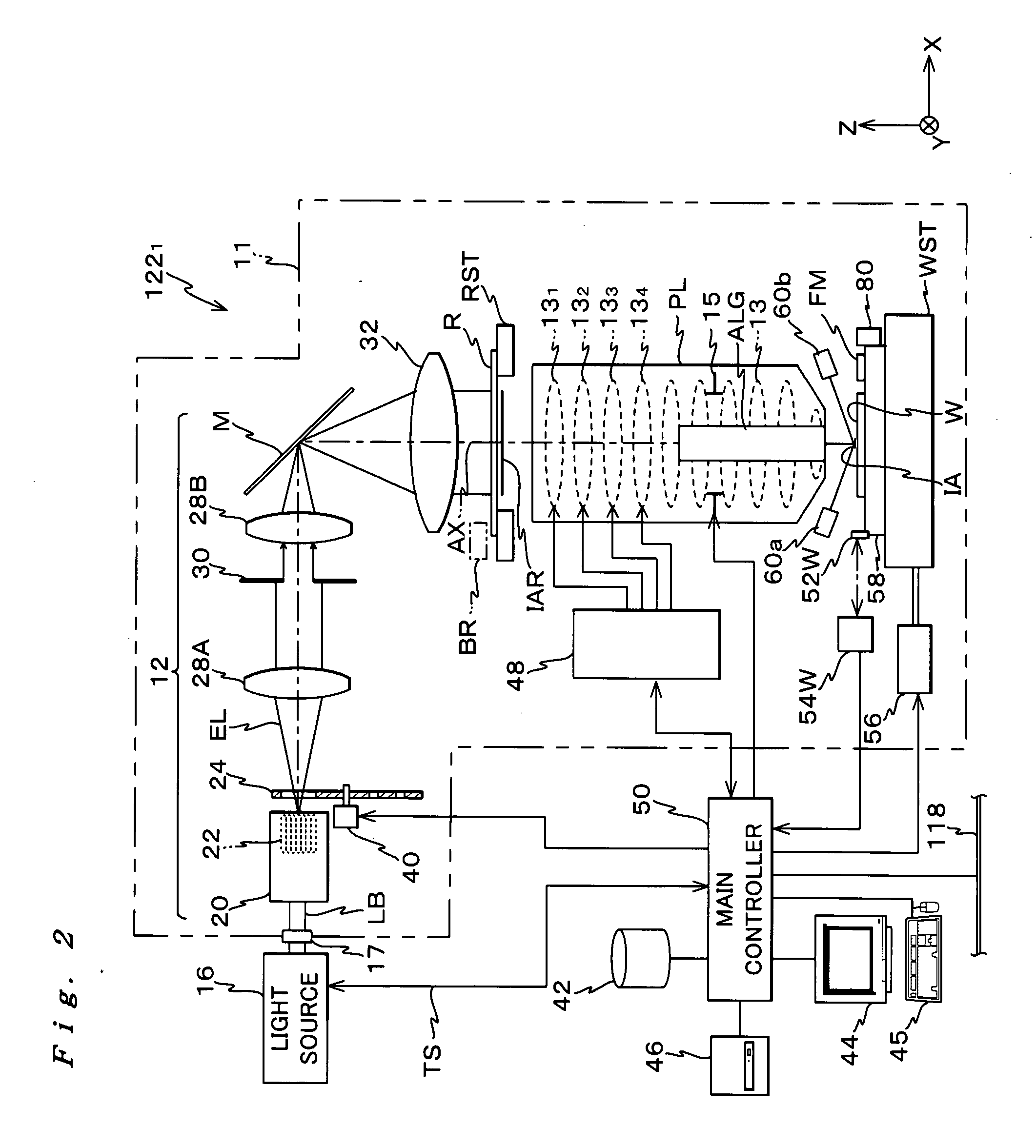
[0053] An embodiment of the present invention will be described below based on FIGS. 1 to 14.

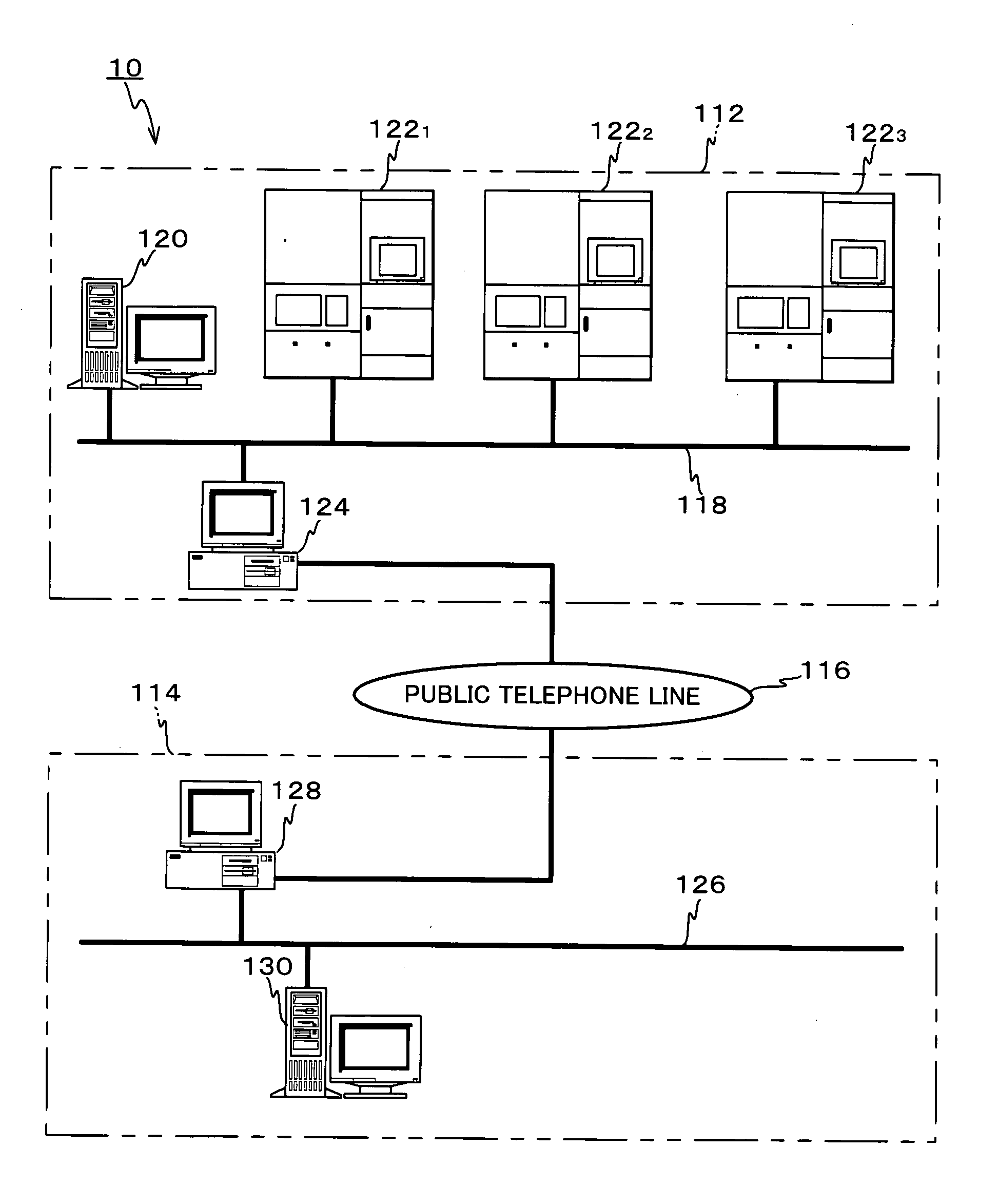
[0054]FIG. 1 shows the schematic construction of a computer system according to an embodiment of this invention.

[0055] A computer system 10 shown in FIG. 1 comprises a lithography system 112 in a semiconductors-manufacturing factory of a device maker (hereinafter, called “maker A” as needed), which is a user of a device manufacturing apparatus such as an exposure apparatus, and a computer system 114 of an exposure apparatus maker (hereinafter, called “maker B” as needed) connected via a communication line including public telephone line 116 to part of lithography system 112.

[0056] Lithography system 112 comprises a first communication server 120 as a first computer, a first, second and third exposure apparatuses 1221, 1222, 1223 as optical apparatuses, a first proxy server 124 for verification, and the like, all of which are connected with each other via a local area network (LAN) 118.

[0...


PUM


Abstract

An exposure apparatus comprises: a movable body that is arranged on an image plane side with respect to a projection optical system; a wavefront measuring unit at least a part of which is arranged on the movable body and that measures wavefront information of the projection optical system; an adjusting unit that adjusts an imaging state of a projected pattern generated on an object via the projection optical system; and a controller that determines adjustment information of the projection optical system using the least-squares method based on the wavefront information and Zernike Sensitivity corresponding to exposure conditions of the object, and controls the adjusting unit based on the adjustment information. The controller determines a coefficient in a predetermined term of a Zernike polynomial from the wavefront information, and determines an adjustment amount of an optical element of the projection optical system as the adjustment information, based on data regarding a relation between an adjustment amount of the optical element of the projection optical system and variation of the determined coefficient in a predetermined term of a Zernike polynomial.

Description

CROSS-REFERENCE TO RELATED APPLICATIONS [0001] This application is a continuation-in-part of U.S. application Ser. No. 11 / 214,795, filed Aug. 31, 2005, which is a divisional of Ser. No. 10 / 072,866, filed Feb. 12, 2002, the disclosure of each is hereby incorporated herein by reference in their entirety. This application also claims the benefit under 35 USC §119 of Japanese applications nos. 2001-036182, filed Feb. 13, 2001, 2001-036184, filed Feb. 13, 2001, 2001-051178, filed Feb. 26, 2001, 2002-023547, filed Jan. 31, 2002 and 2002-023567, filed Jan. 31, 2002, the disclosure of each is herein incorporated by reference.BACKGROUND OF THE INVENTION [0002] 1. Field of the Invention [0003] The present invention relates to an exposure apparatus and an exposure method, and a device manufacturing method, and more specifically to an exposure apparatus and an exposure method that is used in a lithography process to manufacture semiconductor devices or the like, and a device manufacturing metho...

Claims


Application Information

Patent Timeline
Patent Type & Authority Applications(United States)
IPC IPC(8): G03B27/52
CPCG03F7/70258G03F7/7085G03F7/706
Inventor HAMATANI, MASATOTSUKAKOSHI, TOSHIO
Owner NIKON CORP
Why Eureka
Try Eureka