Pattern forming method, device, method of manufacture thereof, electro-optical apparatus, and electronic apparatus

a technology of pattern forming and pattern, which is applied in the direction of conductive pattern formation, identification means, instruments, etc., can solve the problems of large scale equipment, difficult to stably form fine patterns, and high manufacturing costs, and achieve accurate and stably form active matrix substrates.

Active Publication Date: 2005-02-03
138 EAST LCD ADVANCEMENTS LTD
View PDF8 Cites 64 Cited by
  • Summary
  • Abstract
  • Description
  • Claims
  • Application Information

AI Technical Summary

Benefits of technology

[0013] In this aspect, the functional liquid is disposed in a region sectioned by the banks and the functional liquid is dried so that a predetermined pattern is formed on the substrate. In this case, since the shape of the pattern is defined by the banks, then by appropriately forming the banks for example, by making the width between adjacent banks narrower, the pattern can be made finer with thinner lines.
[0043] According to these aspects, it becomes possible to accurately and stably form an active matrix substrate having a thin linear pattern.

Problems solved by technology

This photolithography method requires large scale equipment such as vacuum apparatus and complicated steps.
Moreover, the efficiency of using material is only a few percent, and hence most of the material is wasted, resulting in high manufacturing cost.
In the pattern forming method using the abovementioned droplet discharge method, since the discharged droplet spreads out on the substrate after landing, it has been difficult to stably form a fine pattern.
Particularly, in the case where the pattern becomes a conductive film, the liquid is trapped (bulged) due to the spread of the droplet, causing concern of defects such as disconnection or short-circuit.
However, recently, it has been found that if the functional liquid partially contacts with the top surface of the bank, a fine residue remains on the top surface of the bank.

Method used


Image

  • Pattern forming method, device, method of manufacture thereof, electro-optical apparatus, and electronic apparatus
  • Pattern forming method, device, method of manufacture thereof, electro-optical apparatus, and electronic apparatus
  • Pattern forming method, device, method of manufacture thereof, electro-optical apparatus, and electronic apparatus

Examples


first embodiment

[0071] (First Embodiment)

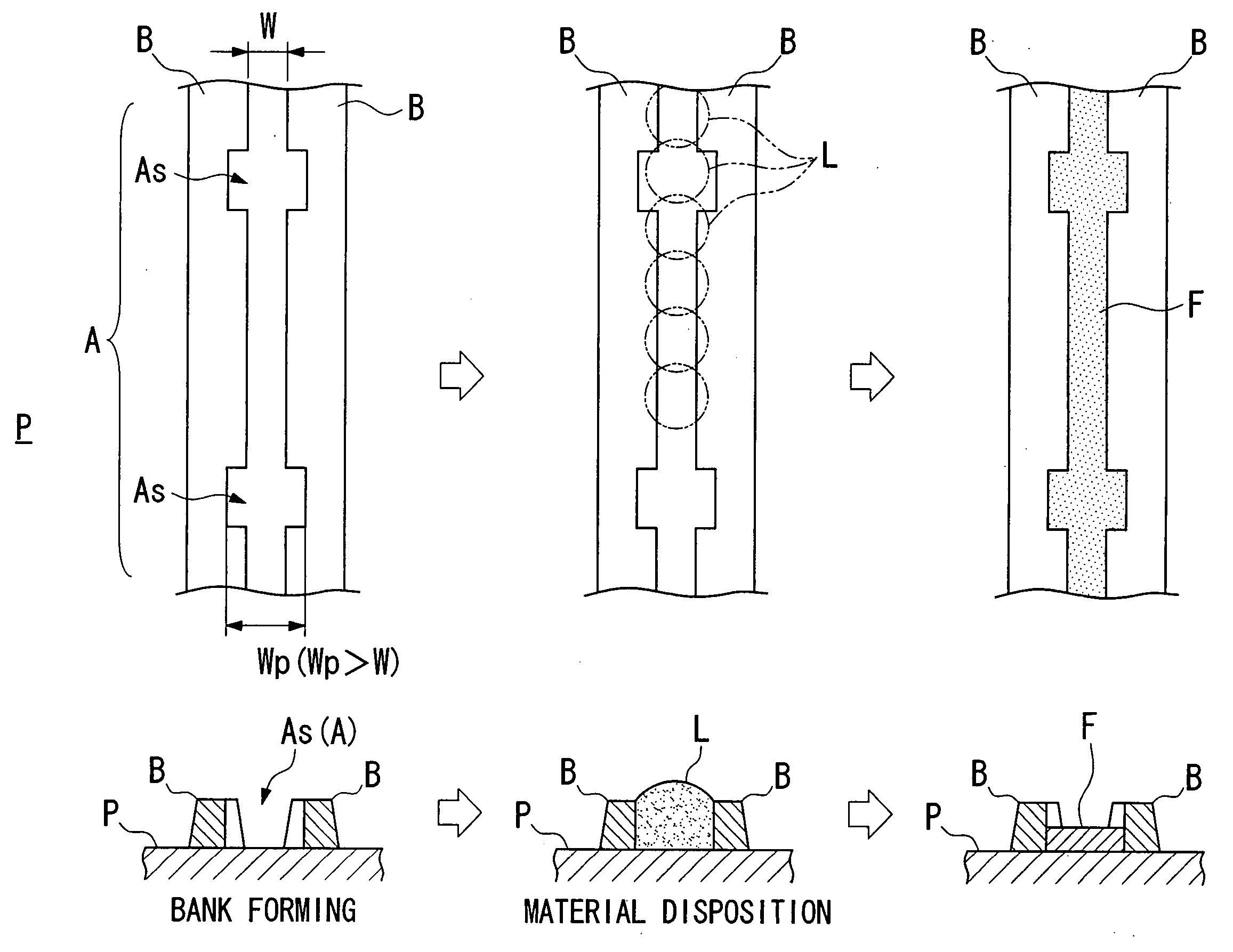
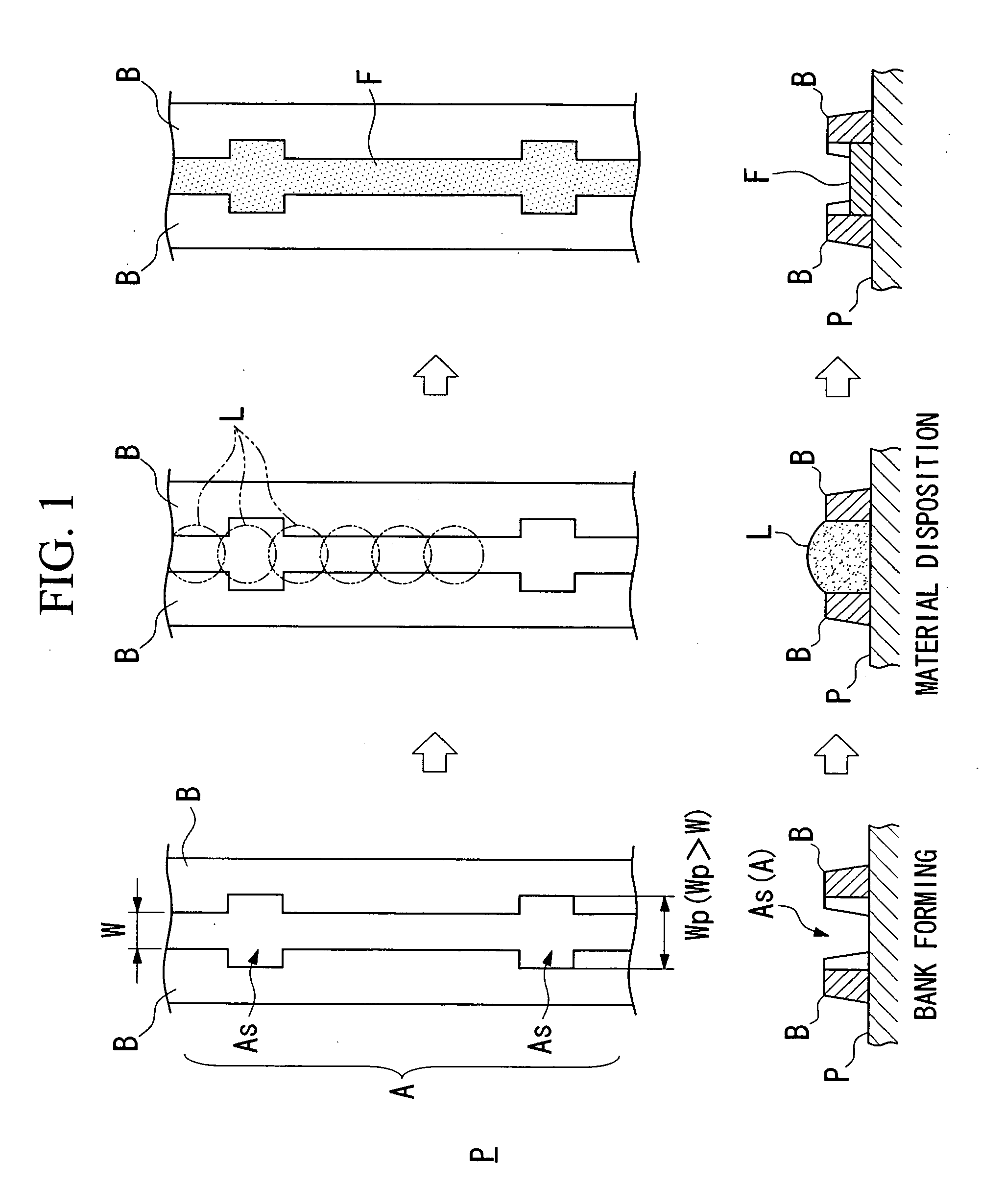
[0072]FIG. 1 is a schematic diagram showing a pattern forming method of the present invention.

[0073] The pattern forming method of the present invention includes a bank forming step for forming banks B on a substrate P, and a material disposition step of disposing a functional liquid L in a linear region “A” sectioned by the banks B.

[0074] In the pattern forming method of the present invention, this functional liquid L is disposed in a linear region A sectioned by the banks B, and the functional liquid L is dried so that a linear pattern F is formed on the substrate P. In this case, since the shape of the pattern F is defined by the banks B, by appropriately forming the banks B, for example by making the width between the adjacent banks B narrower, the pattern F can be made finer with thinner lines. After forming the pattern F, the banks B may be removed from the substrate P, or may remain on the substrate P as is.

[0075] Moreover, in the pattern forming m...

second embodiment

[0155] (Second Embodiment)

[0156] Next is a description of a second embodiment of a wiring pattern forming method of the present invention, with reference to FIG. 8.

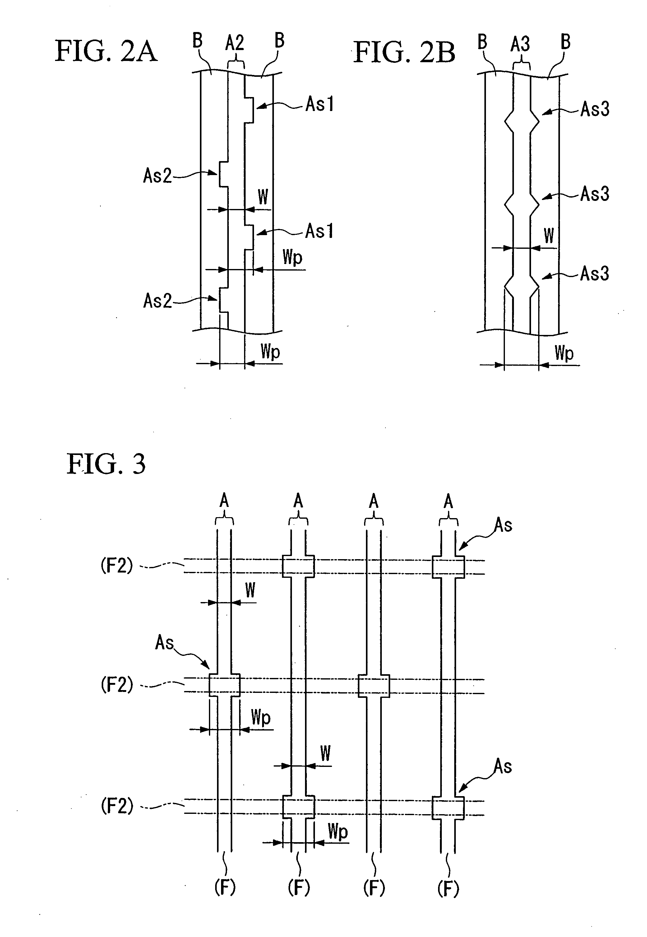
[0157]FIG. 8 is a schematic diagram for explaining the wiring pattern forming method according to the present embodiment. Here, in the following description, the same reference symbols are used for components the same or equivalent to those in the abovementioned embodiment, and description thereof is simplified or omitted.

[0158] In FIG. 8, on a substrate P, a first ditch section 34A (broad width section) having a first width H1 due to the banks B, and a second ditch section 34B (narrow width section) for connecting with the first ditch section 34A and having a second width H2 are formed. The first width H1 is formed larger than the diameter of the functional liquid in flight. The second width H2 is narrower than the first width H1. In other words, the second width H2 is less than the first width H1. Moreover, the first ...


PUM

PropertyMeasurementUnit
diameteraaaaaaaaaa
surface tensionaaaaaaaaaa

Abstract

A method of forming a predetermined pattern by disposing a functional liquid on a substrate, the method includes the steps of forming banks on the substrate, and disposing the functional liquid on a region divided by the banks, wherein a width of the region is partially formed so as to be large.

Description

BACKGROUND OF THE INVENTION [0001] 1. Field of the Invention [0002] The present invention relates to a pattern forming method, a device, a method of manufacture thereof, an electro-optical apparatus, and electronic apparatus. [0003] Priority is claimed on Japanese Patent Application No. 2003-151284, filed May 28, 2003, and Japanese Patent Application No. 2004-124211, filed Apr. 20, 2004, the contents of which are incorporated herein by reference. [0004] 2. Description of Related Art [0005] As a method of forming a wiring pattern used for electronic circuits, integrated circuits, or the like, for example, a photolithography method has been used. This photolithography method requires large scale equipment such as vacuum apparatus and complicated steps. Moreover, the efficiency of using material is only a few percent, and hence most of the material is wasted, resulting in high manufacturing cost. [0006] With respect to this, as shown for example in Japanese Unexamined Patent Applicatio...

Claims


Application Information

Patent Timeline
Patent Type & Authority Applications(United States)
IPC IPC(8): B05D1/26H05B33/10G02F1/1345G09F9/30H01L21/288H01L21/3205H01L21/336H01L21/48H01L21/768H01L21/77H01L21/84H01L27/12H01L27/32H01L29/417H01L29/786H01L51/00H01L51/50H01L51/56H05K3/12
CPCH01L21/4867Y10T29/49117H01L27/12H01L27/3295H01L29/41733H01L29/66765H01L29/78669H01L51/0005H01L51/0022H01L51/56H05K3/125H05K2201/09727H05K2201/09909H01L27/1292Y10T29/49155Y10T29/49126H01L21/76838H10K59/122H10K71/135H10K71/611H10K71/00G02F1/1345
Inventor HIRAI, TOSHIMITSUMIKOSHIBA, TOSHIAKI
Owner 138 EAST LCD ADVANCEMENTS LTD
Why Eureka
Try Eureka