Forming method of contact hole, and manufacturing method of semicondutor device, liquid crystal display device and EL display device

a technology of liquid crystal display and contact hole, which is applied in the direction of semiconductor devices, instruments, electrical devices, etc., can solve the problems of contact defects, reduced throughput, and inability to process the entire surface of the display panel at a time by one exposure step, so as to achieve cost reduction, high yield, and simplify the effect of forming steps

Inactive Publication Date: 2005-08-04
SEMICON ENERGY LAB CO LTD
View PDF33 Cites 59 Cited by
  • Summary
  • Abstract
  • Description
  • Claims
  • Application Information

AI Technical Summary

Benefits of technology

[0009] In view of the foregoing problems, the invention provides a forming method of an excellent contact hole as well as an interlayer film, a planarizing film and an insulating film such as a gate insulating film that are provided in the periphery thereof by a simplified step. Further, the invention provides a manufacturing method of a semiconductor device, which is low in cost and high in throughput and yield.
[0019] In particular when PVA is used, the mask pattern can be easily removed by H2O. When polyimide or acryl is used, the mask pattern can be easily removed by a stripper such as “Nagase resist strip N-300” (product of Nagase ChemteX Co., Ltd., hereinafter referred to as an N300 stripper) that contains as main components 2-amino ethanol and glycol ether, and “Stripper 710” (product of Tokyo Ohka Kogyo Co., ltd., hereinafter referred to as a 710 stripper) that contains as main components o-dichlorobenzene, phenol, and alkyl benzene sulfonate. Needless to say, the mask pattern may be removed by ashing or etching These removing methods can also be adopted in the case where the mask pattern is patterned as is in conventional technologies.
[0040] According to the invention, an organic film having liquid repellency to an insulating material used for an interlayer insulating film, a planarizing film, a gate insulating film and the like is selectively formed in an area over a semiconductor layer, a conductive layer or an insulating layer, in which a contact hole is to be formed. Then, insulating films are formed around the organic film, thereby these insulating films can be formed in a desired area and a contact hole can be formed between the insulating films in a self-aligned manner. In addition, the contact hole and the insulating films can be formed without exposure and development steps that require a resist masks Thus, forming steps can be considerably simplified as compared with conventional steps.
[0041] Further, when a gate electrode, a mask pattern, a conductor and the like are formed by a droplet discharge method, a droplet containing a material of these films can be discharged in an arbitrary area by changing the relative position between a substrate and a nozzle for discharging a droplet. The thickness and the width of a pattern to be formed can be adjusted by the nozzle diameter, the discharge amount of droplet, and relative relationship between the movement speeds of the nozzle and the substrate to be applied with the droplet. Thus, the material of the films can be accurately discharged to form the films in a predetermined area. In addition, since a patterning step, that is exposure and development steps using a resist mask can be omitted, significant simplification of the forming steps and the cost reduction can be attempted. Further, by using the droplet discharge method, patterns can be formed in an arbitrary area and the thickness and the width of the patterns to be formed can be adjusted. Therefore, even a-large semiconductor clement substrate with a side of 1 to 2 m can be manufactured with high yield and at low cost.
[0042] As set forth above, a contact hole and an insulating film around the contact hole in a semiconductor device can be accurately formed by simple steps. Further, it is possible to provide a manufacturing method of a semiconductor device, which is low in cost and high in throughput and yield.

Problems solved by technology

When the size of a substrate increases, however, an entire surface of a display panel cannot be processed at a time by one exposure step.
However, in the case of forming a contact hole by a conventional manufacturing step of a semiconductor device, a resist is required to be formed on almost entire surface of a substrate so as to be applied on a film other than an area in which a contact hole is formed, leading to drastically reduced throughput.
Even when throughput is improved, in the case where the amount of the resist being applied and the surface quality of a base film are not sufficiently controlled, the contact hole is also covered with the resist and contact defects may occur.

Method used


Image

  • Forming method of contact hole, and manufacturing method of semicondutor device, liquid crystal display device and EL display device
  • Forming method of contact hole, and manufacturing method of semicondutor device, liquid crystal display device and EL display device
  • Forming method of contact hole, and manufacturing method of semicondutor device, liquid crystal display device and EL display device

Examples


embodiment mode 1

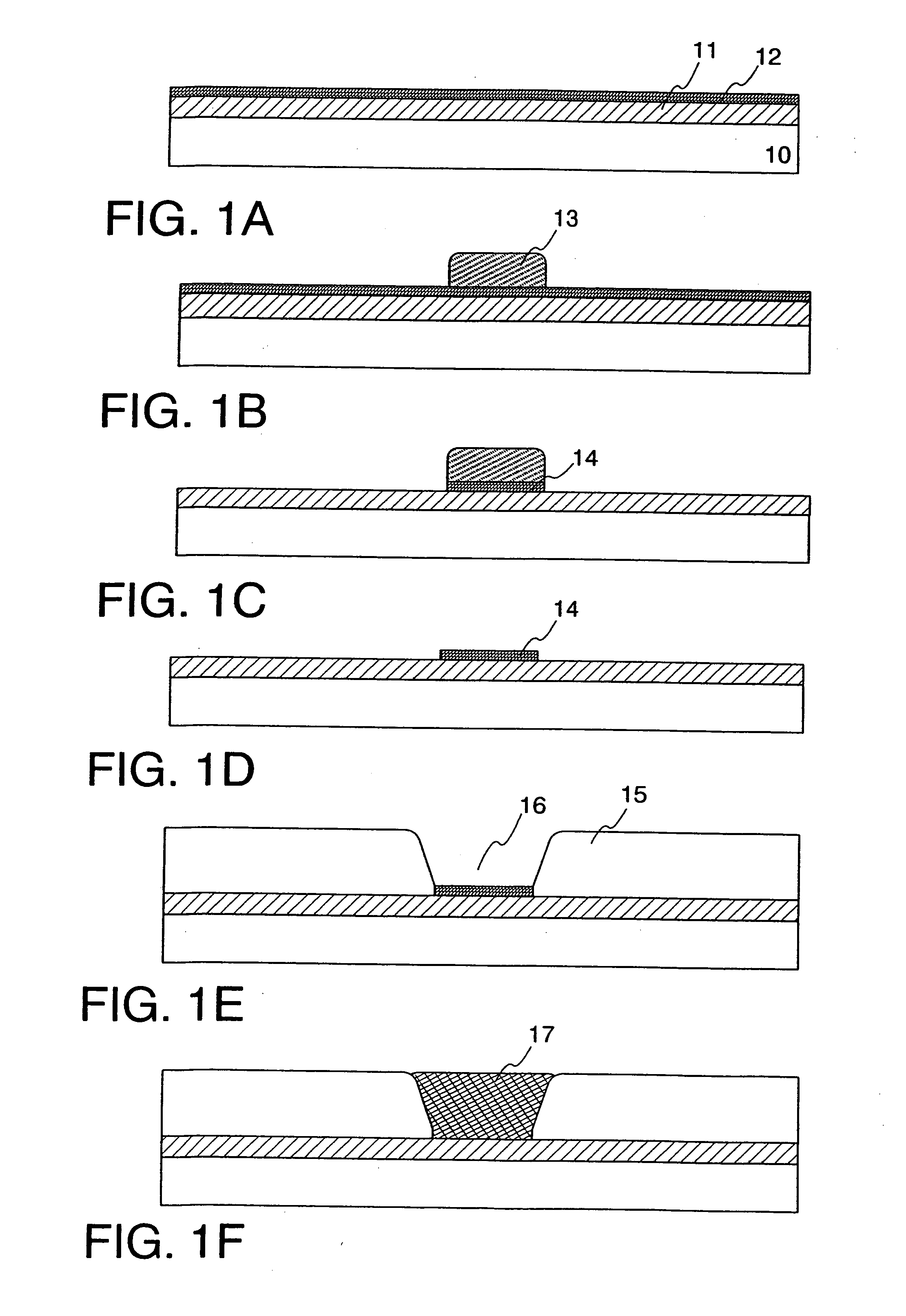
[0071] In this embodiment mode, a forming method of a contact hole according to the invention is described with reference to FIGS. 1A to 1F.

[0072] First, a conductive or semiconductor film 11 is formed over a substrate 10, and then an organic film 12 is applied on an entire surface of the substrate 10 by spin coating, slit coating or the like (FIG. 1A). The organic film 12 is typically formed of a fluorine-based silane coupling agent such as fluoroalkyl silane, though the invention is not limited to this.

[0073] Next, a mask pattern 13 is selectively formed in an area in which a contact hole is to be formed (FIG. 1B). It is desirable to form the mask pattern 13 selectively by a droplet discharge method. The mask pattern 13 is formed of a water soluble resin such as PVA (polyvinyl alcohol) or an organic resin such as polyimide, acryl and siloxane, though the invention is not limited to this.

[0074] Then, the organic film 12 is removed using the mask pattern 13 as a mask, thereby an ...

embodiment mode 2

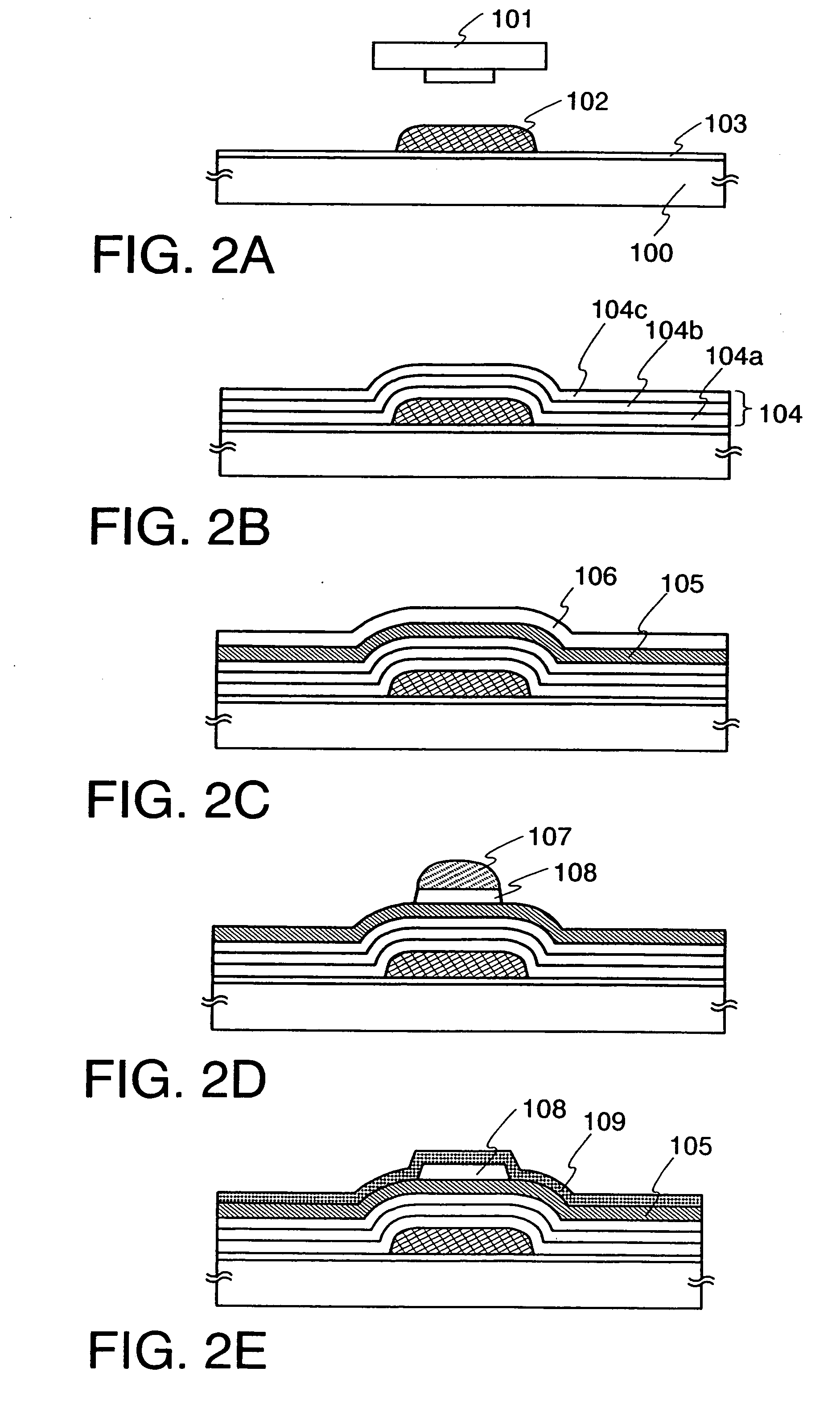
[0080] In this embodiment mode, a manufacturing method of a bottom gate TFT according to the invention, in particular a manufacturing method of a channel protected TFT is described with reference to FIGS. 2A to 2E and FIGS. 3F to 3I.

[0081] First, base film pretreatment is applied to an area over a substrate, in which at least a gate electrode is to be formed. In this embodiment mode, a titanium oxide (TiOx) film 103 is formed over an entire surface of a substrate 100 (FIG. 2A). This pretreatment allows to increase the adhesiveness between the substrate 100 and a conductive film (a gate electrode 102 herein) that is to be formed later by discharging a composition containing a conductive material. When a titanium oxide film is formed, light transmissivity can be increased. Instead of titanium oxide, polyimide, acryl or a heat resistant resin such as siloxane may be used as well. Alternatively, plasma treatment may be performed.

[0082] It is also possible to use a photocatalytic subst...

embodiment mode 3

[0133] In this embodiment mode, a manufacturing method of a bottom gate TFT according to the invention, in particular a manufacturing method of a channel etched TFT is described with reference to FIGS. 4A to 4D and FIGS. 5E to 5G.

[0134] A gate electrode 402, a gate insulating film 404 and a semiconductor film 405 can be formed over a substrate 400 in the same manner as that described in Embodiment Mode 2 (see FIG. 4A and FIGS. 2A to 2C). In this embodiment mode, the base film pretreatment such as the formation of a titanium oxide film is omitted. However, it is needless to say that the pretreatment may be performed similarly to Embodiment Mode 2. Further, although the gate insulating film 404 has a single layer structure, it may have a multi-layer structure. Note that since a channel protective film is not provided in this embodiment mode, a mask pattern corresponding to the first mask pattern in Embodiment Mode 2 is not required.

[0135] An N-type semiconductor film 409 is formed o...


PUM


Abstract

When forming a contact hole by a conventional manufacturing step of a semiconductor device, a resist is required to be formed on almost entire surface of a substrate so as to be applied on a film other than an area in which a contact hole is to be formed, leading to drastically reduced throughput. According to a forming method of a contact hole and a manufacturing method of a semiconductor device, an EL display device and a liquid crystal display device of the invention, an island shape organic film is selectively formed over a semiconductor layer, a conductive layer or an insulating layer, and an insulating film is formed around the island shape organic film to form a contact hole. Therefore, a conventional patterning using a resist is not required, and high throughput and low cost can be achieved.

Description

BACKGROUND OF THE INVENTION [0001] 1. Field of the Invention [0002] The present invention relates to a manufacturing method of a semiconductor device, a liquid crystal display device and an EL display device using a droplet discharge method typified by ink jet printing. In particular, the invention relates to a forming method of a contact hole provided in the semiconductor device. [0003] 2. Description of the Related Art [0004] In the manufacture of semiconductor devices, liquid crystal display devices or EL display devices, it has been suggested that a droplet discharge apparatus is used to form thin films and wiring patterns in order to reduce the equipment cost and simplify the steps. [0005] In such a case, a contact hole of a semiconductor device is formed by the steps of prebaking a resist applied on an entire surface of a substrate, forming a resist pattern by photolithography in which UV rays and the like are irradiated through a mask and developed, and etching and removing a...

Claims


Application Information

Patent Timeline
Patent Type & Authority Applications(United States)
IPC IPC(8): H01L29/786H01L21/336H01L21/77H01L21/84H01L27/12H01L29/423H01L29/49
CPCH01L27/12H01L29/42384H01L27/1292H01L29/66757H01L29/66765H01L29/4908H01L29/41733H01L29/458H01L27/124H01L27/1248G02F1/136227G02F1/136286H10K59/123
Inventor FUJII, GENSHIROGUCHI, HIROKO
Owner SEMICON ENERGY LAB CO LTD
Why Eureka
Try Eureka