P-channel field-effect transistor with reduced junction capacitance

a field-effect transistor and junction capacitance technology, applied in the field of field-effect transistors, can solve the problems of difficult to reliably control typical commercially available state-of-the-art ion-implantation equipment, and achieve the effect of reducing junction capacitance and increasing igfet switching speed

Inactive Publication Date: 2006-12-05
NAT SEMICON CORP
View PDF33 Cites 59 Cited by
  • Summary
  • Abstract
  • Description
  • Claims
  • Application Information

AI Technical Summary

Benefits of technology

[0024]The present invention furnishes a p-channel insulated-gate field-effect transistor whose source/drain doping is controlled so that each source/drain zone has a vertically “graded” junction characteristic. That is, in moving upward from the pn junction between a source/drain zone and the adjoining body material, the net dopant concentration in a vertical cross-section through the source/drain zone ri...

Problems solved by technology

With boron being an atom of relatively low molecular weight and with the main source/drain portions being shallower than the lower source/drain portions, one reason for this difference in dopant species is that it is difficult to reliably contro...

Method used


Image

  • P-channel field-effect transistor with reduced junction capacitance
  • P-channel field-effect transistor with reduced junction capacitance
  • P-channel field-effect transistor with reduced junction capacitance

Examples


Embodiment Construction

Reference Notation and Other Conventions

[0075]The reference symbols employed below and in the drawings have the following meanings:

[0076]

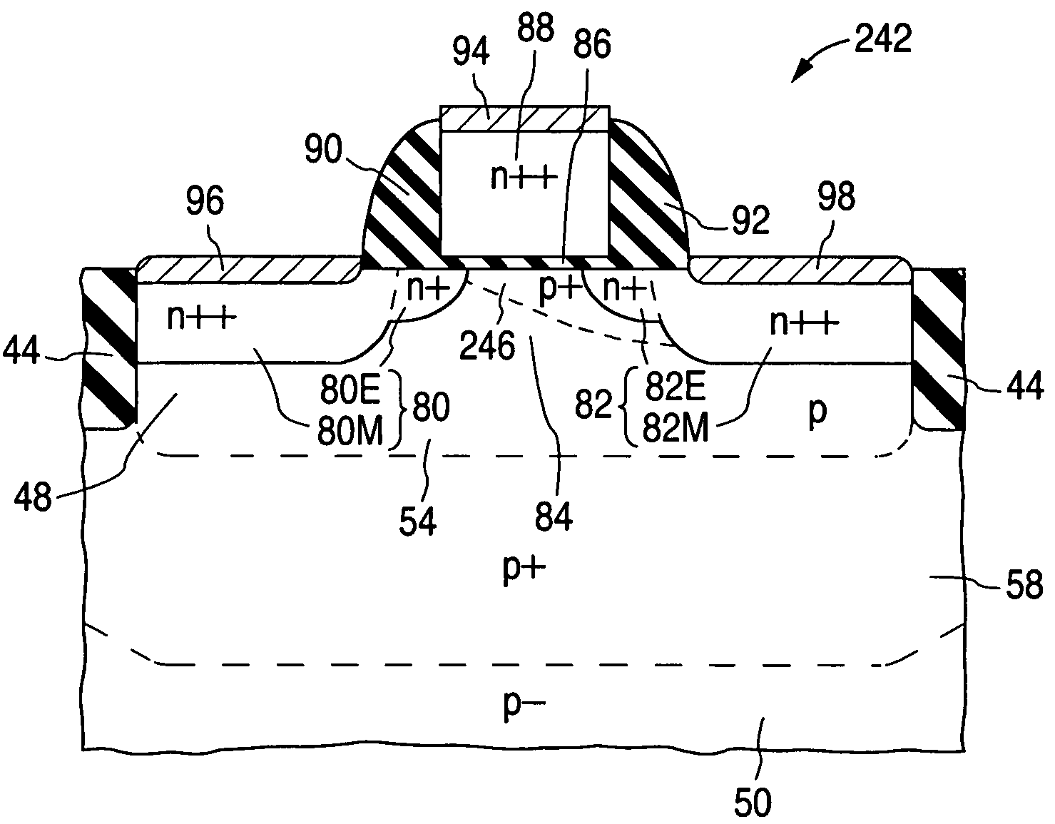
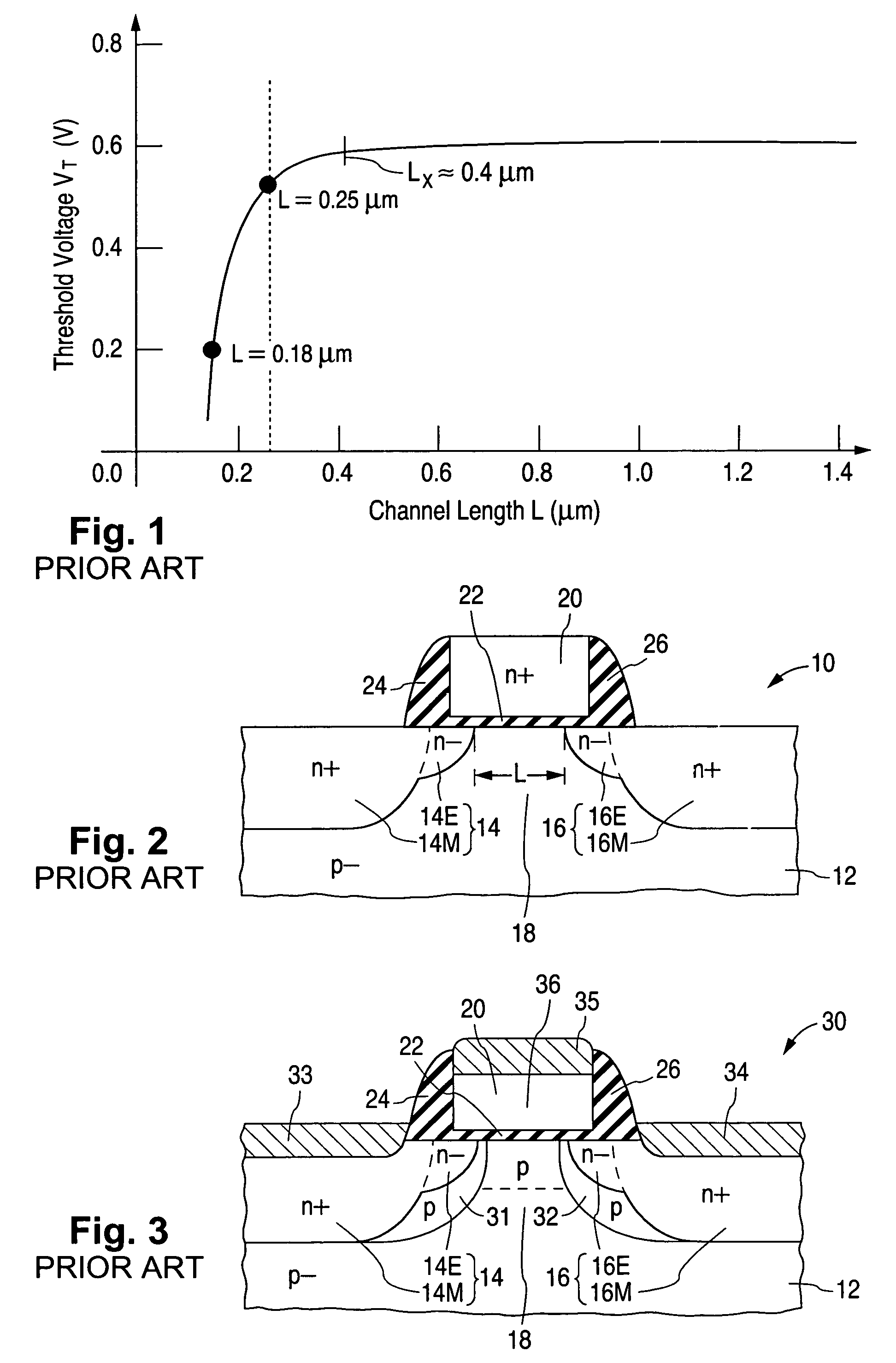
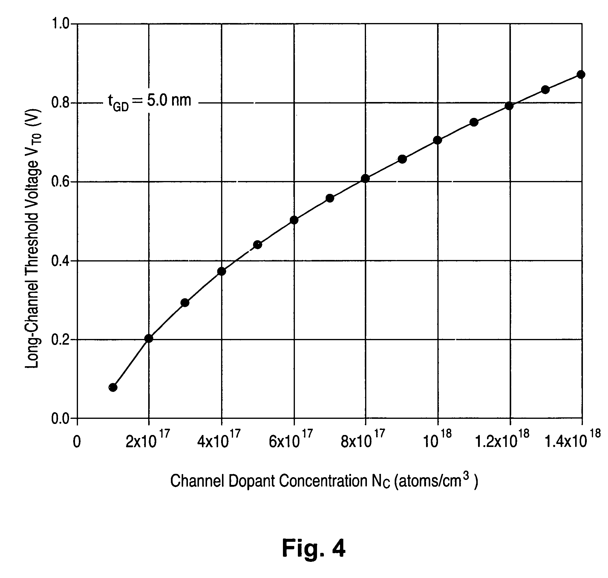
A ≡halo dopant atomAI ≡pair of dopant atom A andinterstitial atom Ia ≡experimentally determinedcoefficientb ≡experimentally determinedcoefficientC(A)TOT ≡total concentration (single andpaired) of dopant atom A in crystalCGD ≡gate dielectric capacitance per unitareaCJ ≡capacitance per unit area of pnjunction between body material andsource / drain zonec ≡lateral distance from gate electrodestructure across location ofsource / drain zone to field-insulation region in direction alongchannel lengthsD(AO) ≡equilibrium diffusion constant ofhalo dopant atoms ADOSEAPT ≡dosage of ions of anti-punchthroughdopantDOSEHalo ≡dosage of ions of halo dopantdG ≡lateral distance between gateelectrode structures in directionalong channel length of IGFETreceiving halo ion implantationdGmin ≡minimum tolerable value of distancedGdM ≡lateral distance from gate electrodestruct...


PUM


Abstract

The source/drain zones (140 and 142 or 160 and 162) of a p-channel IGFET (120 or 122) are provided with graded-junction characteristics to reduce junction capacitance, thereby increasing switching speed. Each source/drain zone contains a main portion (140M, 142M, 160M, or 162M) and a more lightly doped lower portion (140L, 142L, 160L, or 162L) underlying, and vertically continuous with, the main portion.

Description

CROSS-REFERENCE TO RELATED APPLICATIONS[0001]This is a division of U.S. patent application Ser. No. 10 / 327,352, filed 30 Dec. 2002, now U.S. Pat. No. 6,797,576 B1, which is a continuation of U.S. patent application Ser. No. 09 / 947,012, filed 4 Sep. 2001, now U.S. Pat. No. 6,599,804 B2, which is a division of U.S. patent application Ser. No. 09 / 540,442, filed 31 Mar. 2000, now U.S. Pat. No. 6,548,842 B1.FIELD OF USE[0002]This invention relates to semiconductor technology and, in particular, to field-effect transistors (“FETs”) of the insulated-gate type. All of the insulated-gate FETs (“IGFETs”) described below are surface-channel enhancement-mode IGFETs except as otherwise indicated.BACKGROUND[0003]An IGFET is a semiconductor device in which a gate dielectric layer electrically insulates a gate electrode from a channel zone that extends between a source and a drain in a semiconductor body. The channel zone in an enhancement-mode IGFET is part of a body region, commonly termed the su...

Claims


Application Information

Patent Timeline
IPC IPC(8): H01L29/76
CPCH01L21/823807H01L21/823814H01L29/105H01L29/1083
Inventor TENG, CHIH SIEHBULUCEA, CONSTANTINSHYU, CHIN-MIINWANG, FU-CHENGCHAPARALA, PRASAD
Owner NAT SEMICON CORP
Why Eureka
Try Eureka