SOI low capacitance body contact

a low capacitance, body contact technology, applied in the direction of semiconductor devices, electrical apparatus, transistors, etc., can solve the problems of increasing capacitance, increasing the resistance of the junction, so as to reduce the junction capacitance

Inactive Publication Date: 2002-04-09
IBM CORP
View PDF16 Cites 17 Cited by
  • Summary
  • Abstract
  • Description
  • Claims
  • Application Information

AI Technical Summary

Benefits of technology

is to provide a method and structure for making an PET on SOI which reduces junction capacitance.

Problems solved by technology

However, when designing and forming FETs on a silicon-on-insulator structure, where the device is formed over an insulating layer, the body tends to float relative to ground, and threshold voltage, on current, off current and other parameters are variable and not readily determined.
However, there remain problems with undesirable capacitance increases in body contact with the FET which remain unresolved by this proposed solution.
Further problems are expected to occur when shallow trench isolation (STI) is applied to FETS on SOI.

Method used


Image

  • SOI low capacitance body contact
  • SOI low capacitance body contact
  • SOI low capacitance body contact

Examples


Embodiment Construction

)

In describing the preferred embodiment of the present invention, reference will be made herein to FIGS. 1-9 of the drawings in which like numerals refer to like features of the invention. Features of the invention are not necessarily shown to scale in the drawings.

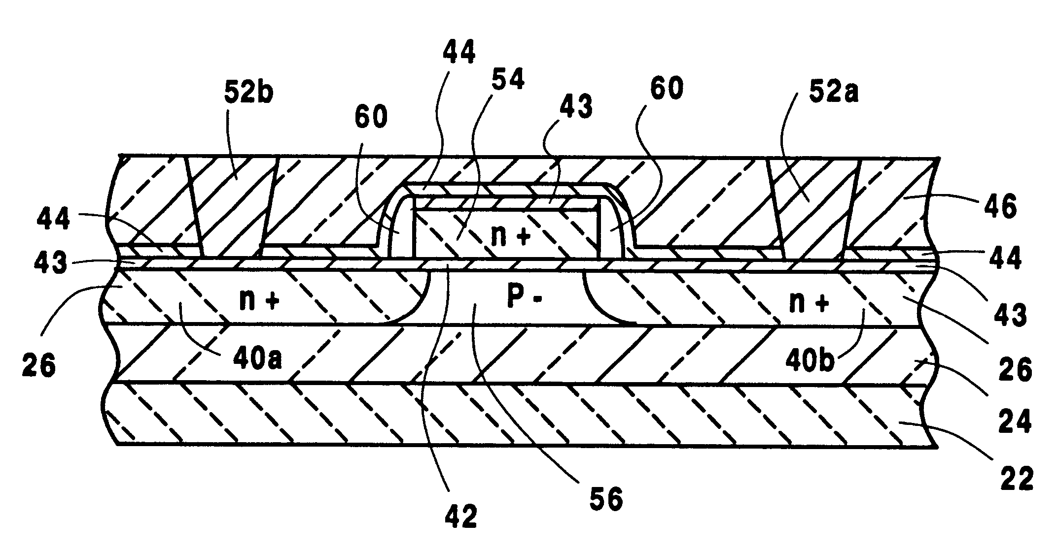
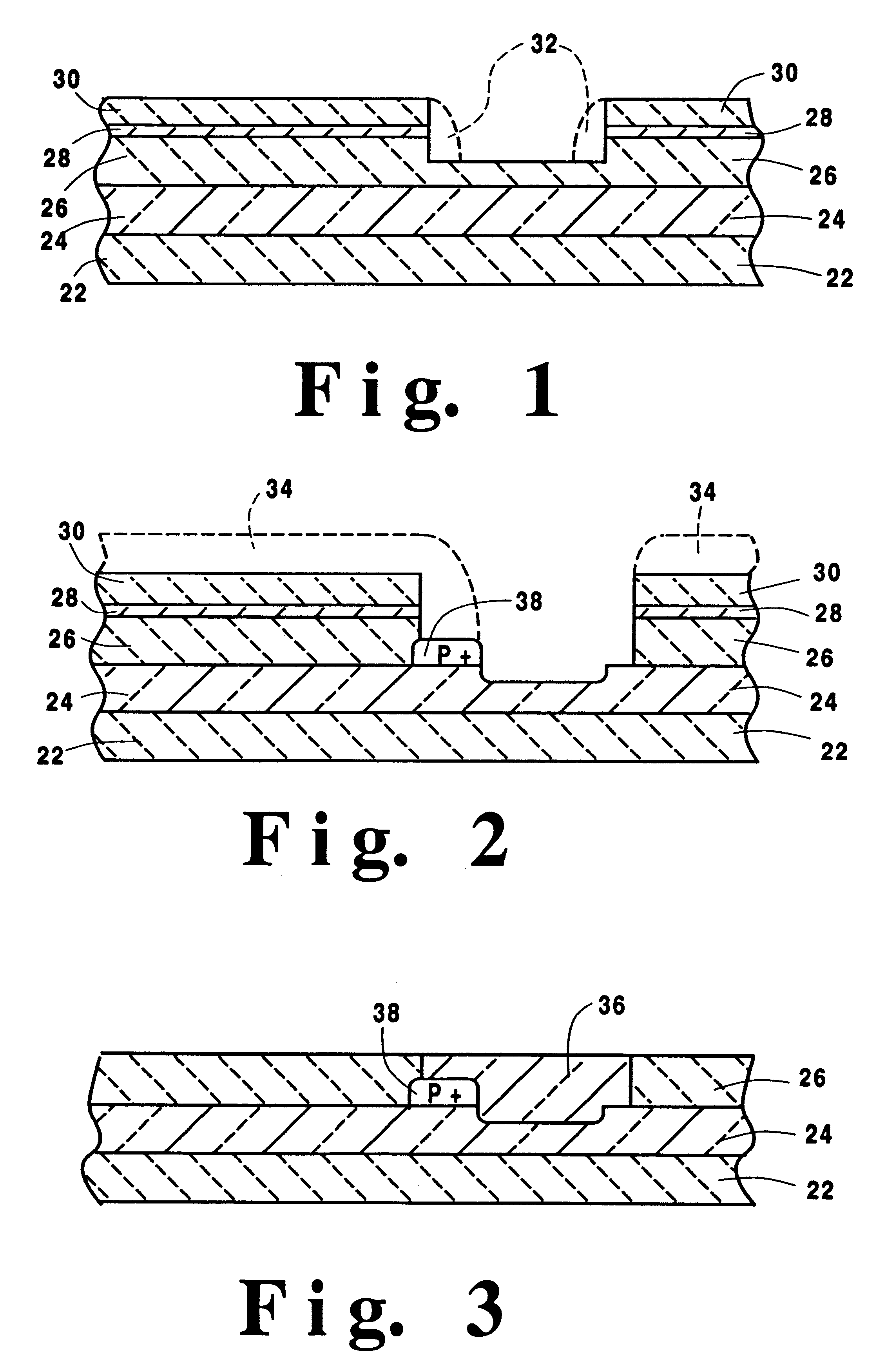
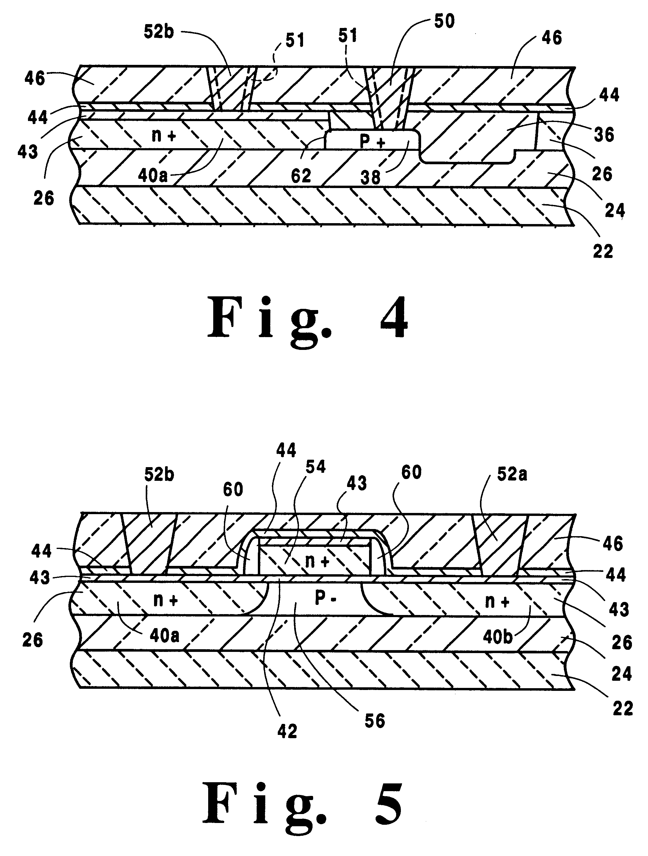
The present invention may be manufactured according to conventional lithographic processing techniques which are well known in the art. In a first stage shown in FIG. 1, there is provided a silicon-on-insulator (SOI) structure comprising a bulk silicon layer 22 over which is deposited, in sequence, a dielectric layer or region 24, preferably of an oxide such as silicon dioxide; and substrate layer or region 26, preferably of polycrystalline silicon. The SOI structure may be obtained in a variety of ways known in the prior art. Preferably, it is obtained by implantation of the oxide layer or bonding of separate layers. In the oxide implantation method, a single crystal substrate wafer is obtained and then implanted with hi...


PUM


Abstract

An FET device and method of making comprising a first dielectric layer; a substrate layer on the dielectric layer; a channel region of a first conductivity type formed in the substrate layer; a gate formed above the substrate layer over the channel region; FET diffusion regions of a second conductivity type formed in the substrate layer, the diffusion regions each having edges, the edges of the FET diffusion regions being separated by the channel region; and a body contact region of the first conductivity type extending continuously from the channel region. The first conductivity type material in the body contact region is thinner than the first conductivity type material in the channel region. The FET also includes a second dielectric layer formed on the body contact region.

Description

1. Field of the InventionThis invention relates to integrated circuit devices using Field Effect Transistors (FETs), and more particularly, to a methods of making the same.2. Description of Related ArtConventional bulk silicon metal oxide semiconductor (MOS) and conductive metal oxide semiconductor (CMOS) technology has the ability to contact the silicon substrate from a relatively great distance away from a structure such as a field effect transistor (FET), e.g., 20-40 microns away, and hold the NFET body at ground potential. Likewise, contact with the n well of, for example, a PFET body may be made at a similar distance and be assured that it will be held at voltage (V.sub.DD). The device then has its own body voltage, and the on current / off current and overall circuit performance can be calculated with relatively great assurance. However, when designing and forming FETs on a silicon-on-insulator structure, where the device is formed over an insulating layer, the body tends to flo...

Claims


Application Information

Patent Timeline
Patent Type & Authority Patents(United States)
IPC IPC(8): H01L21/02H01L29/66H01L21/336H01L29/786
CPCH01L29/78615H01L29/66757
Inventor BRYANT, ANDRESMANN, RANDY W.STAMPER, ANTHONY K.
Owner IBM CORP
Why Eureka
Try Eureka