Semiconductor device and method of manufacturing the same

a technology of semiconductor devices and semiconductors, applied in the field of semiconductor devices and methods of manufacturing the same, can solve the problems of increasing junction leakage and junction capacitance, affecting the effect of junction capacitance, and difficult for the gate to effectively control the bottom of the fin, so as to reduce the junction capacitance and reduce leakage

Active Publication Date: 2015-11-05
INST OF MICROELECTRONICS CHINESE ACAD OF SCI
View PDF3 Cites 17 Cited by
  • Summary
  • Abstract
  • Description
  • Claims
  • Application Information

AI Technical Summary

Benefits of technology

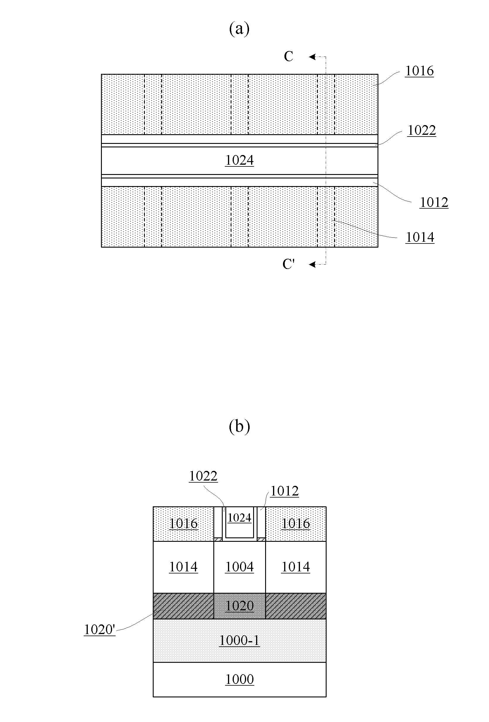
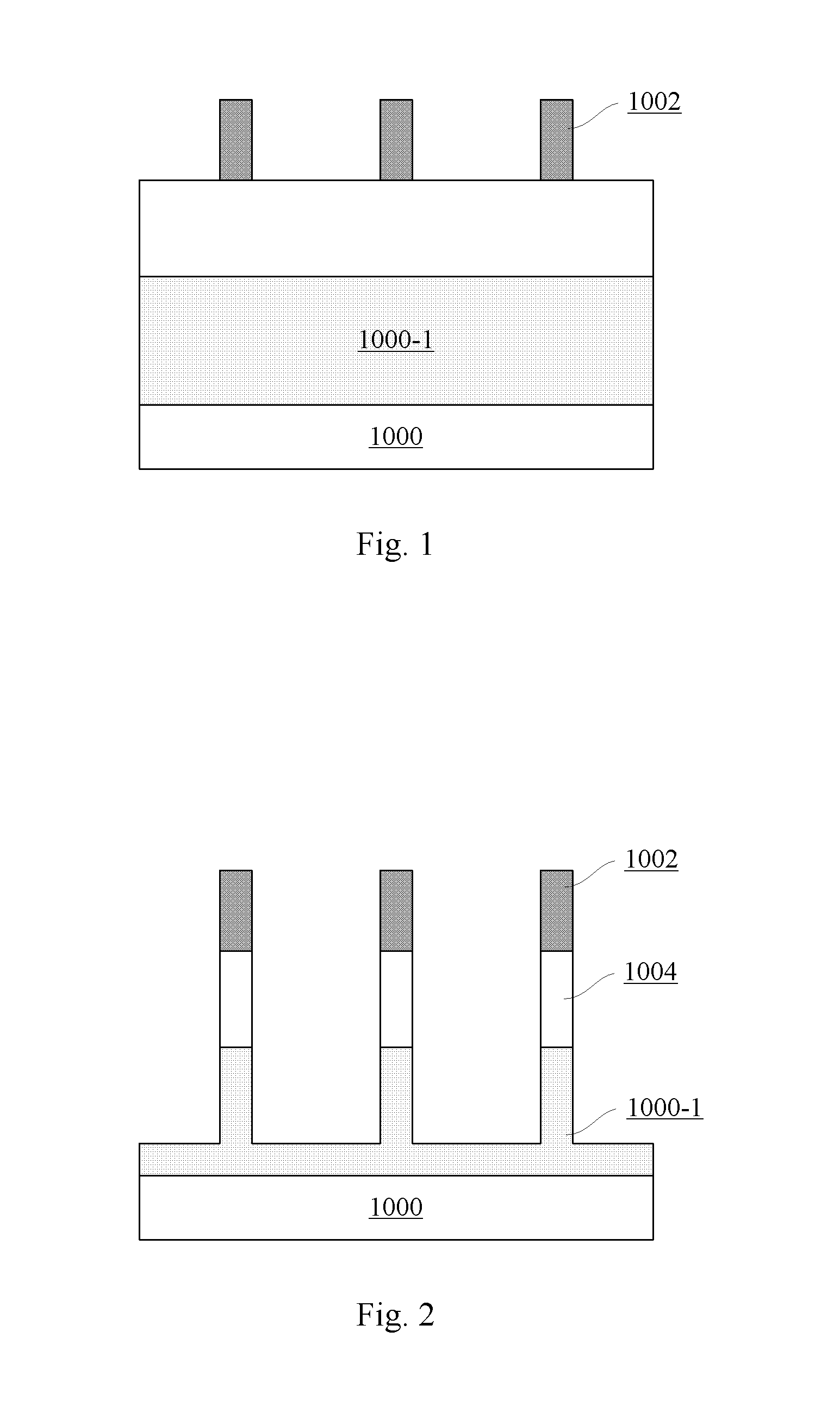
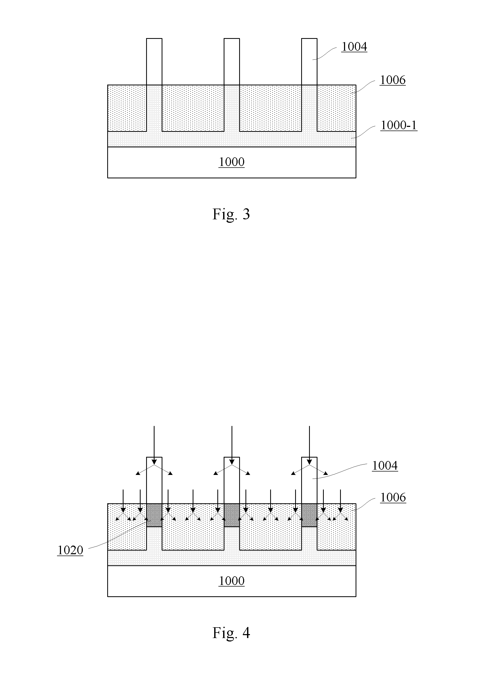
[0008]According to embodiments of the present disclosure, the PTS is formed under the fin. By means of the first ion implantation and the second implantation as described above, the first section of the PTS whose doping concentration is relatively high is self-aligned to and directly under a channel region, and thus it is possible to effectively reduce leakage between source and drain. Further, the second sections of the PTS whose doping concentration is relatively low are self-aligned to and directly under the source and drain, and thus it is possible to reduce a junction capacitance between the source / drain and the substrate.

Problems solved by technology

Therefore, it is difficult for the gate to effectively control the bottom of the fin.
As a result, a leakage current tends to occur between a source and a drain via the bottom of the fin.
However, introduction of such a PTS increases junction leakage and junction capacitance.

Method used


Image

  • Semiconductor device and method of manufacturing the same
  • Semiconductor device and method of manufacturing the same
  • Semiconductor device and method of manufacturing the same

Examples


Embodiment Construction

[0011]Hereinafter, the technology disclosed herein is described with reference to embodiments thereof shown in the attached drawings. However, it should be noted that those descriptions are just provided for illustrative purpose, rather than limiting the present disclosure. Further, in the following, descriptions of known structures and techniques are omitted so as not to obscure the concept of the present disclosure.

[0012]In the drawings, various structures according to the embodiments are schematically shown. However, they are not drawn to scale, and some features may be enlarged while some features may be omitted for sake of clarity. Moreover, shapes and relative sizes and positions of regions and layers shown in the drawings are also illustrative, and deviations may occur due to manufacture tolerances or technique limitations in practice. Those skilled in the art can also devise regions / layers of other different shapes, sizes, and relative positions as desired.

[0013]In the conte...


PUM


Abstract

Provided are a semiconductor device and a method of manufacturing the same. An example device may include: a fin formed on a substrate; a gate stack formed on the substrate and intersecting the fin, wherein the gate stack is isolated from the substrate by an isolation layer, and a Punch-Through Stopper (PTS) formed under the fin, including a first section directly under a portion of the fin where the fin intersects the gate stack and second sections on opposite sides of the first section, wherein the second sections each have a doping concentration lower than that of the first section.

Description

CROSS-REFERENCE TO RELATED APPLICATION[0001]This application is a U.S. national phase application of PCT Application No. PCT / CN2013 / 071636 filed on Feb. 18, 2013, entitled “Semiconductor Device and Method of Manufacturing the Same,” which claimed priority to Chinese Patent Application No. 201310014886.0, filed on Jan. 15, 2013. Both the PCT Application and the Chinese Application are incorporated herein by reference in their entireties.TECHNICAL FIELD[0002]The present disclosure relates to the semiconductor technology, and particularly to semiconductor devices and methods of manufacturing the same.BACKGROUND[0003]Short channel effects are getting more significant as planar semiconductor devices are increasingly scaled down. To this end, three-dimensional (3D) semiconductor devices, such as Fin Field Effect Transistors (FinFETs), have been proposed. Generally, a FinFET includes a fin formed vertically on a substrate and a gate stack intersecting the fin. In addition, an isolation lay...

Claims


Application Information

Patent Timeline
Patent Type & Authority Applications(United States)
IPC IPC(8): H01L29/78H01L29/66H01L21/02H01L29/10H01L29/06H01L21/308H01L29/165H01L21/265
CPCH01L29/7848H01L29/165H01L29/7851H01L29/6681H01L21/0257H01L29/1083H01L29/0638H01L21/3083H01L21/02532H01L21/26513H01L21/823431H01L27/0886H01L29/66545H01L29/66795
Inventor ZHU, HUILONG
Owner INST OF MICROELECTRONICS CHINESE ACAD OF SCI
Why Eureka
Try Eureka