Semiconductor device and method of manufacturing the same

a semiconductor and semiconductor technology, applied in the direction of semiconductor devices, electrical devices, transistors, etc., can solve the problems of increased manufacturing cost, short channel effect in the conventional planar type mosfet, and often decrease the driving force, so as to reduce the width of the active region, reduce the junction capacitance, and advantageously adjust the width of the gate structure

Active Publication Date: 2007-01-23
SAMSUNG ELECTRONICS CO LTD
View PDF8 Cites 16 Cited by
  • Summary
  • Abstract
  • Description
  • Claims
  • Application Information

AI Technical Summary

Benefits of technology

[0009]The present invention provides a fin type MOSFET having improved reliability by reducing a junction capacitance thereof without a short channel effect.
[0010]The present invention also provides a method of manufacturing a fin type MOSFET having improved reliability.
[0012]According to another embodiment of the present invention, a method of manufacturing a semiconductor device comprises forming a field region and an active region in a semiconductor substrate by forming a field layer on the semiconductor substrate. The method further comprises forming gate trench patterns on the semiconductor substrate, wherein the gate trench patterns selectively expose portions of the semiconductor substrate. The method further comprises partially removing portions of the field layer exposed by the gate trench patterns and selectively reducing a width of the active region, wherein a sidewall of the active region is exposed in accordance with a partial removal of the field oxide layer. The method further comprises forming a gate conductive layer on the semiconductor substrate to cover the gate trench patterns and forming gate structures on the substrate by partially removing the gate conductive layer, wherein the gate structures are separated from each other by the gate trench patterns. The method further comprises removing the gate trench patterns.
[0013]According to the present invention, the gate structures of the fin type MOSFET are formed by a damascene process without a photolithography process to thereby advantageously adjust the widths of the gate structures. Additionally, impurities used to form a channel region are selectively implanted into the portions of the substrate adjacent to the gate structures so that the fin type MOSFET may have a reduced junction capacitance.

Problems solved by technology

However, where the channel length is decreased in a conventional MOSFET having a planar structure, the channel driving force often decreases and an electric field caused by a drain voltage have an increased effect on the performance of the MOSFET, thereby causing a short channel effect in the conventional planar type MOSFET.
However, since this fin type MOSFET is formed on a silicon-on-insulator (SOI) substrate, it may have an increased manufacturing cost.
As a result, the MOSFET may be deteriorated due to heat generated therein because the heat is not easily transferred from the body of the MOSFET.
However, a gate structure is typically imprecisely formed on the fin shaped active region due to a relatively high step generated between the fin shaped active region and adjacent portions of the bulk silicon substrate.
Hence, etched residues generated in the etching process for the gate structure typically remain on or near the fin shaped active region, causing an electrical failure of the fin type MOSFET.
Additionally, the junction capacitance of the fin type MOSFET often increases because impurities used to form a channel region are implanted into undesired portions of the bulk silicon substrate.

Method used


Image

  • Semiconductor device and method of manufacturing the same
  • Semiconductor device and method of manufacturing the same
  • Semiconductor device and method of manufacturing the same

Examples


Embodiment Construction

[0023]Exemplary embodiments of the invention are described below with reference to the corresponding drawings. These embodiments are presented as teaching examples. The actual scope of the invention is defined by the claims that follow. It will be understood that when a first element such as a layer, region, or substrate is referred to as being “on” or “onto” second element, the first element is either directly on the second element or is separated from the second element by intervening elements.

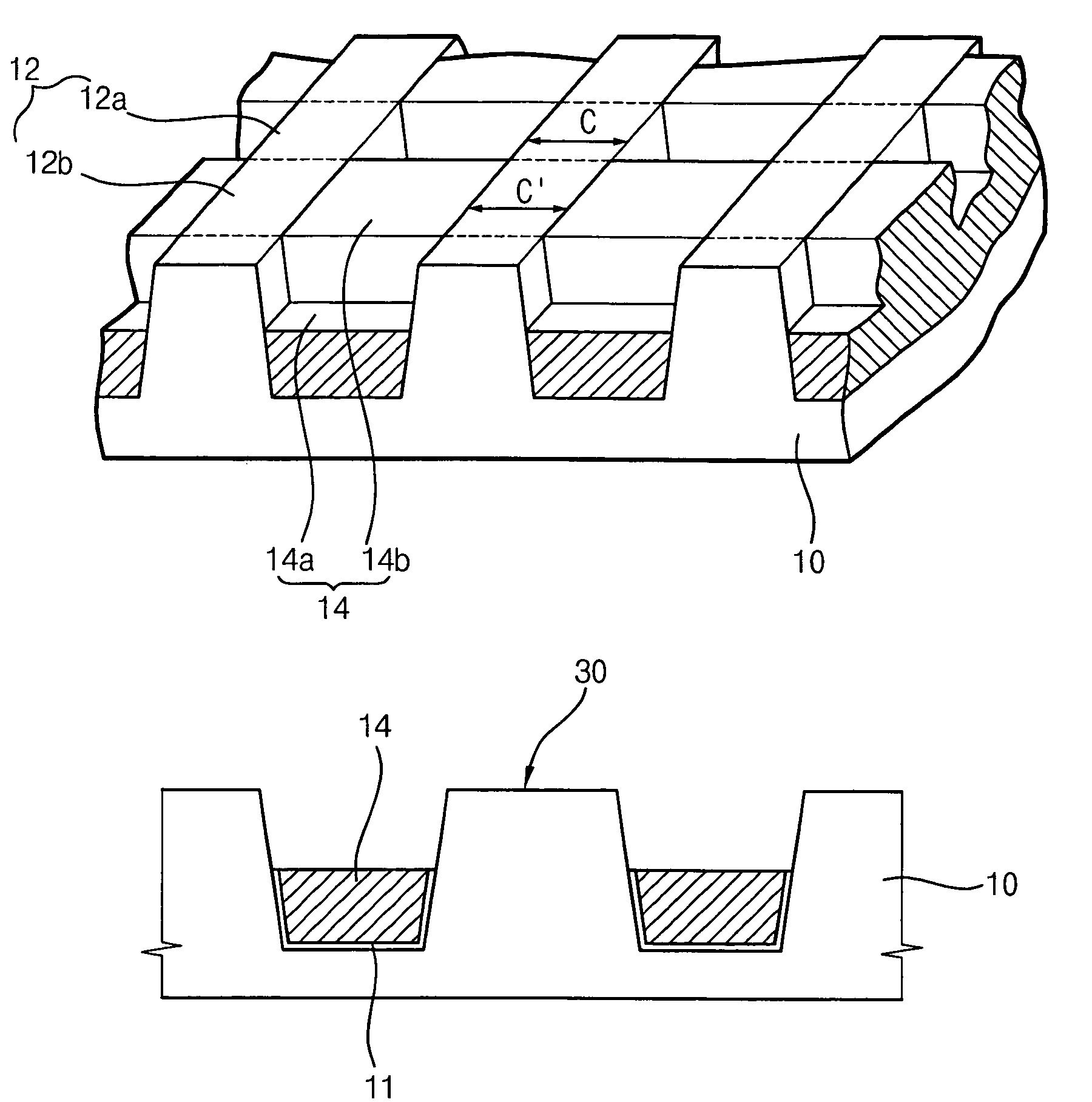
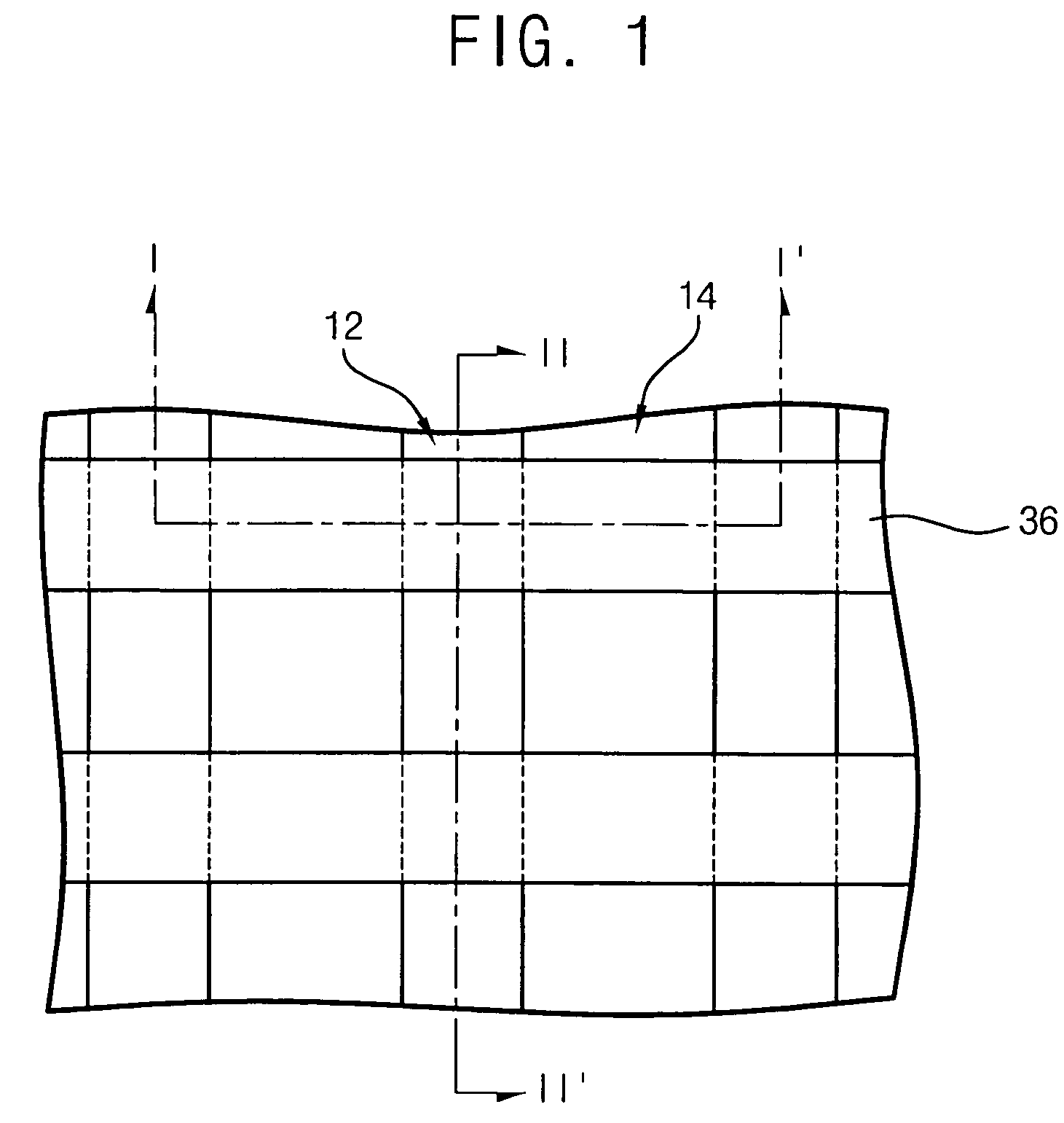
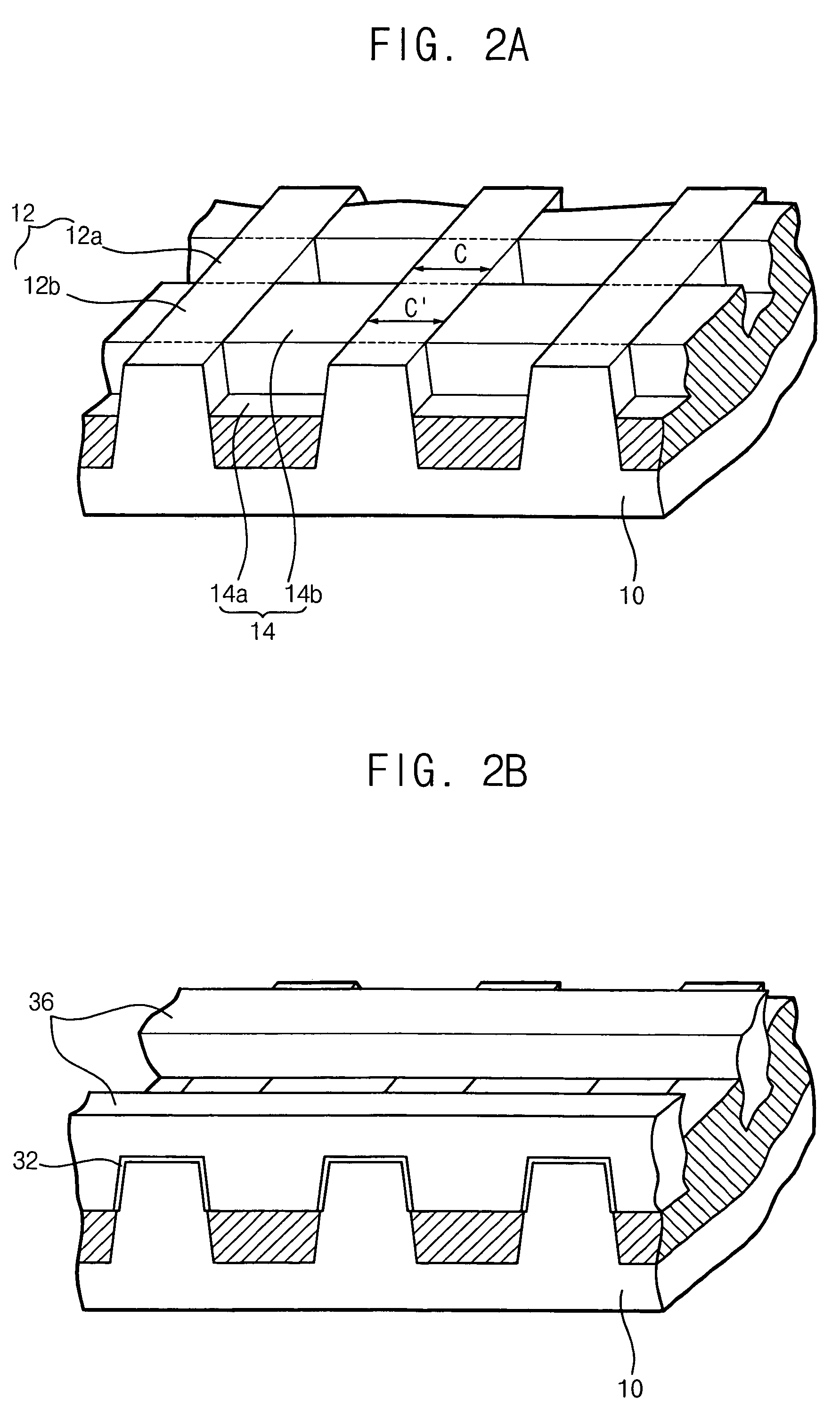
[0024]FIG. 1 is a planar view illustrating a fin type MOSFET in accordance with one embodiment of the present invention, and FIGS. 2A and 2B are perspective views the fin type MOSFET shown in FIG. 1.

[0025]Referring to FIGS. 1, 2A, and 2B, the fin type MOSFET includes a semiconductor substrate 10 divided into an active area 12 and a field area 14. Conductive structures including gate structures, source / drain regions, and a contact, are located in active area 12. Field area 14 isolates conduct...


PUM


Abstract

A fin type MOSFET and a method of manufacturing the fin type MOSFET are disclosed. Gate structures in the fin type MOSFET are formed by a damascene process without a photolithography process. Impurities used to form a channel region are selectively implanted into portions of a semiconductor substrate adjacent to the gate structures.

Description

BACKGROUND OF THE INVENTION[0001]1. Field of the Invention[0002]The present invention relates generally to a semiconductor device and a method of manufacturing the semiconductor device. More particularly, the present invention relates to a fin type metal oxide semiconductor field effect transistor (MOSFET), and a method for manufacturing the fin type MOSFET.[0003]A claim of priority is made to Korean Patent Application No. 10-2004-0006524 filed on Feb. 2, 2004, the disclosure of which is incorporated herein by reference in its entirety.[0004]2. Description of the Related Art[0005]Modern semiconductor devices typically have high response speeds, low power consumptions, and high degrees of integration. MOSFETs commonly use a reduced channel length to attain higher response speeds. However, where the channel length is decreased in a conventional MOSFET having a planar structure, the channel driving force often decreases and an electric field caused by a drain voltage have an increased ...

Claims


Application Information

Patent Timeline
Patent Type & Authority Patents(United States)
IPC IPC(8): H01L21/336H01L29/76H01L29/786
CPCH01L29/7851H01L29/66818Y10S257/90H01L21/18
Inventor KANG, HEE-SOOYOON, JAE-MANPARK, DONG-GUNHAN, SANG-YEONAHN, YOUNG-JOONLEE, CHOONG-HO
Owner SAMSUNG ELECTRONICS CO LTD
Why Eureka
Try Eureka