Method of forming micro pattern in semiconductor device

a technology of semiconductor devices and micro-patterns, which is applied in the direction of semiconductor devices, basic electric elements, electrical appliances, etc., can solve the problems of difficult control of optical proximity correction (opc), the use of x-ray or e-beams has not yet been commercialized, and the variation of cd of the last pattern is difficult to reduce. , to achieve the effect of reducing the variation of cd of the last pattern

Inactive Publication Date: 2007-04-10
SK HYNIX INC
View PDF5 Cites 150 Cited by
  • Summary
  • Abstract
  • Description
  • Claims
  • Application Information

AI Technical Summary

Benefits of technology

[0009]The invention provides a method of forming a micro pattern in a se

Problems solved by technology

However, the use of X-ray or E-beam has not yet been commercialized due to technical problems, productivity, etc.
In practice, since the overlay accuracy of the exposure apparatus is difficult to control t

Method used


Image

  • Method of forming micro pattern in semiconductor device
  • Method of forming micro pattern in semiconductor device
  • Method of forming micro pattern in semiconductor device

Examples


Embodiment Construction

[0023]The invention will now be described in connection with preferred embodiments with reference to the accompanying drawings.

[0024]Since preferred embodiments are provided for the purpose that the ordinary skilled in the art are able to understand the invention, they may be modified in various manners and the scope of the invention is not limited by the preferred embodiments described later.

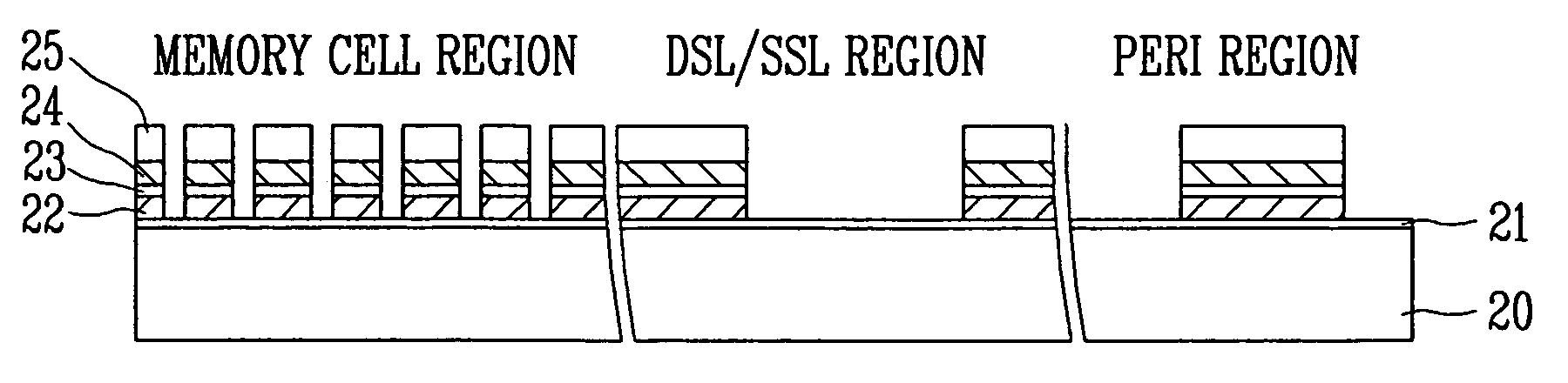
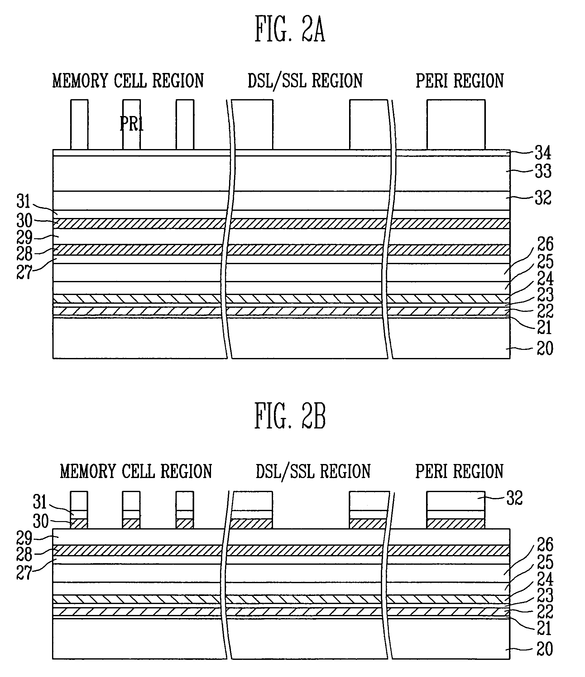
[0025]FIGS. 2a to 2k are cross-sectional view illustrating a process of forming a micro pattern in a semiconductor device according to an embodiment of the invention. FIG. 2 shows an example in which the invention is applied to the gate etch process of a flash memory device.

[0026]Referring first to FIG. 2a, a tunnel oxide film 21 (i.e., a to-be-etched layer), a floating gate conduction film 22, a dielectric film 23, a control gate conduction film 24 and a hard mask nitride film 25 are sequentially formed on a semiconductor substrate 20 hard memory cell region where a memory cell transistor will...


PUM


Abstract

A method of forming a micro pattern in a semiconductor device, wherein a first polysilicon film, a buffer oxide film, a second polysilicon film, an anti-polishing film, and a first oxide film are sequentially laminated on a semiconductor substrate having a to-be-etched layer. The first oxide film, the anti-polishing film and the second polysilicon film are patterned. After nitride film spacers are formed on the patterned lateral portions, a second oxide film is formed on the entire structure. A Chemical Mechanical Polishing (CMP) process is performed using the anti-polishing film as a stopper. Thereafter, after the nitride film spacers are removed, the second oxide film and the second polysilicon film are removed using a difference in etch selective ratio between the oxide film and the polysilicon film. A hard mask for forming a micro pattern having a structure in which the first polysilicon film and the buffer oxide film are laminated is formed. The to-be-etched layer is etched using the hard mask as an etch barrier.

Description

BACKGROUND OF THE INVENTION[0001]1. Field of the Invention[0002]The invention relates generally to a method of manufacturing semiconductor devices and, more particularly, to a method of forming a micro pattern in a semiconductor device, in which a micro pattern has a pitch lower than the resolution capability of the exposure apparatus.[0003]2. Discussion of Related Art[0004]In manufacturing semiconductor devices, the minimal pitch of a pattern formed in the photolithography process is determined by the waveform of exposure radiation used. Therefore, to form patterns having smaller pitch as semiconductor devices become increasingly integrated, radiation having a waveform shorter than that of the radiation that is currently used must be used. To this end, it may be preferred that X-ray or E-beam be used. However, the use of X-ray or E-beam has not yet been commercialized due to technical problems, productivity, etc. In view of the above, a Dual Exposure and Etch Technology (DEET) has ...

Claims


Application Information

Patent Timeline
IPC IPC(8): H01L21/311
CPCH01L21/0337H01L21/0338H01L21/32139H01L27/105H01L27/11526H01L27/11546H10B41/49H10B41/40H01L21/31051
Inventor JUNG, WOO YOUNGCHO, SUNG YOONKIM, CHOI DONGSONG, PIL KEUN
Owner SK HYNIX INC
Why Eureka
Try Eureka