Method for correcting critical dimension variations in photomasks

a critical dimension and photomask technology, applied in the field of photomasks, can solve the problems of lithography process suffering from cd variations, often exceeding specifications and requirements, slow process, etc., and achieve the effect of reducing the cd variations in the intra-field field

Active Publication Date: 2007-03-22
PIXER TECH
View PDF6 Cites 41 Cited by
  • Summary
  • Abstract
  • Description
  • Claims
  • Application Information

AI Technical Summary

Benefits of technology

[0016] It is an object of the present invention to provide a way that greatly reduces intra field CD variations associated with a photomask in the photolithographic process.

Problems solved by technology

However, it is well known throughout the semiconductor industry, that the lithography process suffers from CD variations, which often exceed specifications and requirements.
However, such a method is limited in its dynamic range, the process is slow, and suffers from high equipment cost.
There are other methods for CD control, which are commonly used in the semiconductors industry (like the focus / exposure (dose) process-window optimization, which determines the average CD on wafers) but are generally not suitable for controlling CD variations within and across the exposure fields on the wafer (Intra field CD variations).

Method used


Image

  • Method for correcting critical dimension variations in photomasks
  • Method for correcting critical dimension variations in photomasks
  • Method for correcting critical dimension variations in photomasks

Examples


Embodiment Construction

[0037] Process variations in lithographic printing of integrated circuits is characterized by variations in the sizes of lines and spaces printed on Silicon wafers.

[0038] Variations of lines and spaces are measured as average CD (critical dimension) size at different areas on the wafers. If variations in the width of lines and spaces imprinted on a wafer occur, than the photomask is said to have CD variations.

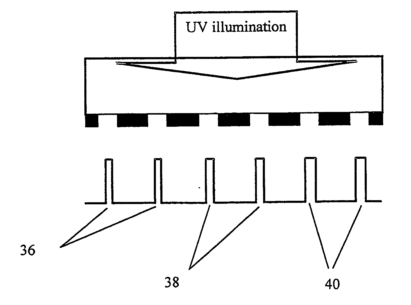
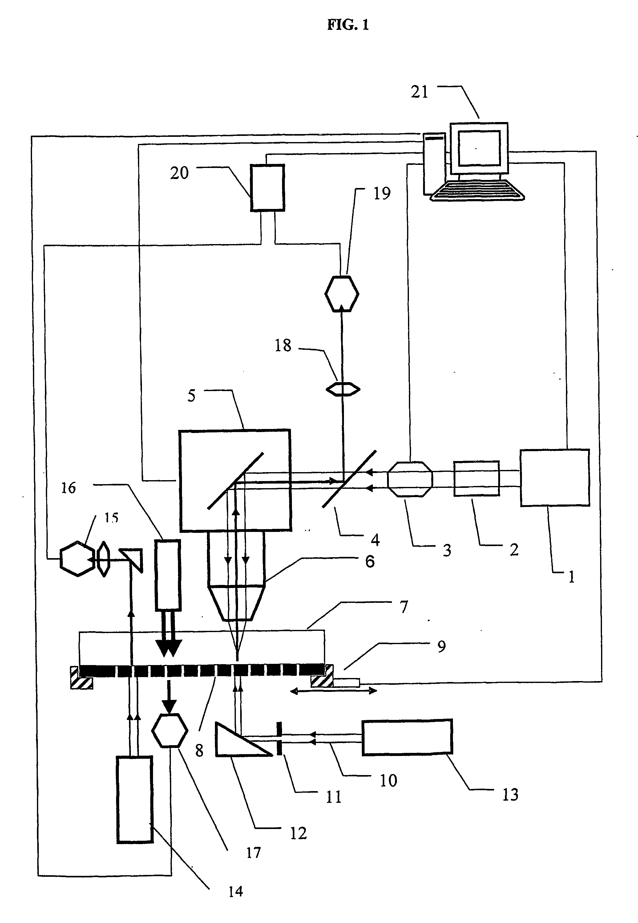
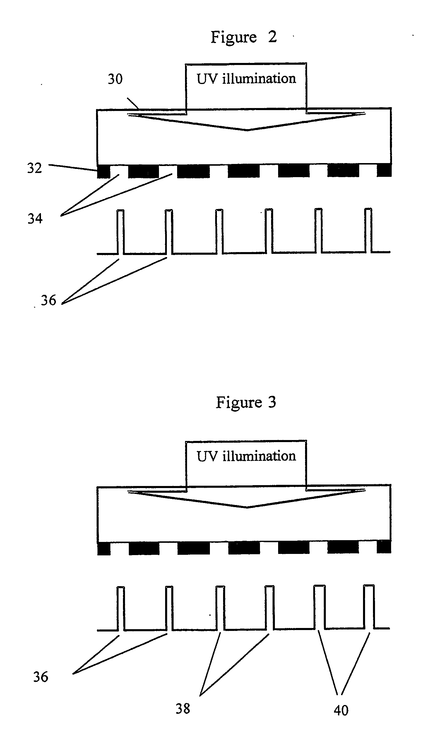
[0039] The present invention provides a novel method for controlling CD variations on the exposure field of a wafer by writing shading elements made of pixels inside the glass substrate of a photomask with an ultrafast femto second laser. The shading element attenuation level is determined by controlling pixel size and pixel 3 dimensional arrangement in the volume of the substrate.

[0040] The required attenuation level is determined by the degree of CD variation from the target CD within the exposure filed of the wafer.

[0041] Attenuating the light passing through a photomask...


PUM

PropertyMeasurementUnit
thicknessaaaaaaaaaa
transparentaaaaaaaaaa
energyaaaaaaaaaa

Abstract

A method for compensating for critical dimension (CD) variations of pattern lines of a wafer, by the correcting the CD of the corresponding photomask. The photomask comprises a transparent substrate having two substantially opposite surfaces, a first back surface and a second front surface on which front surface an absorbing coating is provided, on which the pattern lines were formed by removing the coating at the pattern lines. The method comprises: determining CD variations across regions of a wafer exposure field relating to the photomask; and providing Shading Elements (SE) within the substrate of the photomask in regions which correlates to regions of the wafer exposure field where CD variations greater than a predetermined target value were determined, whereby the shading elements attenuate light passing through the regions, so as to compensate for the CD variations on the wafer and hence provide and improved CD tolerance wafer.

Description

FIELD OF THE INVENTION [0001] The present invention relates to photo-masks. More particularly it relates to a method for treating a photomask to correct critical dimensions (CD) variations in wafers manufactured using that photomask, by way of providing shading elements and or diffractive optical elements for radiation attenuation incorporated in a photo-mask. BACKGROUND OF THE INVENTION [0002] Photo-masks used in the manufacturing of integrated circuits (IC) are composed of a Chrome layer deposited on Quartz or fused Silica plates, which are subsequently patterned for use as a “negative”, similarly to the printing process in photography, in a photolithographic process. [0003] In a photolithographic process, UV (ultraviolet) light passes through the pattern inscribed on the Chrome layer, and an image is formed within the photo-resist layer on top of a Silicone wafer. [0004] Additional layers, like protective layers, antireflective layers, or an embedded phase-shifting layer, such as...

Claims


Application Information

Patent Timeline
Patent Type & Authority Applications(United States)
IPC IPC(8): G03C5/00G03F1/00G03F
CPCG03F1/144G03F7/70433G03F1/54G03F1/38G03F1/50G03F1/70G03F7/20
Inventor ZAIT, EITANDMITRIEV, VLADIMIRGULETSKY, NIKOLAY N.OSHEMKOV, SERGEYBEN-ZVI, GUY
Owner PIXER TECH
Why Eureka
Try Eureka