Method and apparatus employing integrated metrology for improved dielectric etch efficiency

a technology of dielectric etching and integrated metrology, which is applied in the direction of semiconductor/solid-state device testing/measurement, instruments, and therapeutics, etc., can solve the problems of affecting the performance of finished semiconductor devices, unable to measure important parameters, and unable to achieve photoresist loss, so as to reduce cd variations in semiconductor wafers and reduce throughput

Inactive Publication Date: 2007-09-04
APPLIED MATERIALS INC
View PDF34 Cites 14 Cited by
  • Summary
  • Abstract
  • Description
  • Claims
  • Application Information

AI Technical Summary

Benefits of technology

[0014]An advantage of the present invention is the ability to reduce CD variations in semiconductor wafers without reducing throughput, by utilizing information gathered during in-process inspection of the wafers.
[0015]According to the present invention, the foregoing and other advantages are achieved in part by a method of processing a semiconductor wafer, comprising forming an underlying layer on the wafer and a patterned layer on the underlying layer; measuring a dimension of a pattern on the patterned layer and the thickness of the underlying layer at a plurality of different predetermined locations on the wafer; selecting a first set of process parameter values for a process to be performed on the wafer, based on the measurements of the dimension and the thickness; performing the process on the wafer at a processing tool using the first set of process parameter values; measuring a dimension of a structure formed in the underlying layer by the process at the predetermined locations; and selecting a second set of process parameter values for a subsequently processed wafer using the measurements of the structure.
[0016]Another aspect of the present invention is an apparatus for processing a semiconductor wafer, comprising a measuring tool for measuring the thickness of an underlying layer formed on the wafer and a dimension of a pattern on a patterned layer formed on the underlying layer at a plurality of different predetermined locations on the wafer; a processing tool for performing a process on the wafer using a first set of process parameter values; and a processor configured to select the first set of process parameter values based on the measurements of the dimension and the thickness.
[0017]A still further aspect of the present invention is an apparatus for processing a semiconductor wafer, comprising a measuring tool for measuring the thickness of an underlying layer formed on the wafer and a profile and CD of a pattern on a patterned layer formed on the underlying layer at a plurality of different predetermined locations on the wafer; a processing tool for performing a process on the wafer using a first set of process parameter values; a transfer mechanism for transferring the wafer between the measuring tool and the processing tool; a chamber for enclosing the transfer mechanism and allowing communication between the transfer mechanism, the measuring tool and the processing tool in a clean environment; and a processor configured to select the first set of process parameter values based on the measurements of the pattern CD and profile and the underlying layer thickness. The measuring tool is for measuring a CD of a structure formed in the underlying layer by the process at the predetermined locations, and the processor is further configured to select a second set of process parameter values for a subsequently processed wafer using the CD measurements of the structure.
[0018]Additional advantages of the present invention will become readily apparent to those skilled in this art from the following detailed description, wherein only exemplary embodiments of the present invention are shown and described, simply by way of illustration of the best mode contemplated for carrying out the present invention. As will be realized, the present invention is capable of other and different embodiments, and its several details are capable of modifications in various obvious respects, all without departing from the invention. Accordingly, the drawings and description are to be regarded as illustrative in nature, and not as restrictive.

Problems solved by technology

Deviations of a feature's CD and profile from design dimensions may adversely affect the performance of the finished semiconductor device.
Furthermore, the measurement of a feature's CD and profile may indicate photolithography problems, such as stepper defocusing and photoresist loss due to overexposure, and / or etch problems such as improper gas flow and magnetic field intensity.
Although conventional SEM's are useful for measuring CD's, they cannot measure some important parameters, such as thickness of a layer to be etched, and they generally do not provide “real time” metrology.
In other words, they do not provide immediate feedback to the photolithography process, or feed-forward to the etcher, to reduce LTL variations.
SEM measurement is performed “off-line” because it is relatively slow and typically needs to be performed at a separate review station, with inspection results not being known for hours afterward.
Consequently, the results of conventional SEM inspections are not typically used to adjust subsequent etch processing, so the CD measurement of a particular wafer is not used to decide what etch recipe should be used to process that wafer.
As a result, yield is typically low due to an undesirably large amount of scrap.
Moreover, as wafer sizes increase to 300 mm diameter and larger, the amount of scrap grows exponentially with metrology delays if a process problem occurs.
This exposes the wafers to the ambient atmosphere, which can result in unwanted oxidation of the wafer surface or deposition of foreign particles on the surface, thereby lowering yield.
Moreover, etch uniformity across the wafer is not monitored by the interferometric sensor, since only the center dies are “seen” by the sensor.
Therefore, dies away from the center may be improperly etched, and the interferometric sensor cannot be used to monitor or correct this situation.

Method used


Image

  • Method and apparatus employing integrated metrology for improved dielectric etch efficiency
  • Method and apparatus employing integrated metrology for improved dielectric etch efficiency
  • Method and apparatus employing integrated metrology for improved dielectric etch efficiency

Examples


Embodiment Construction

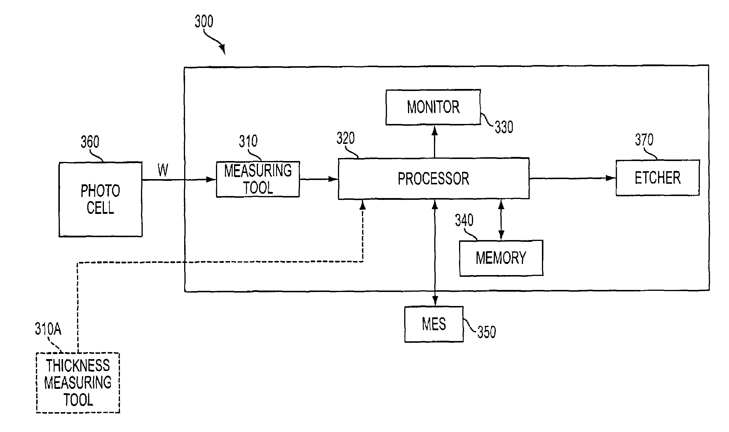
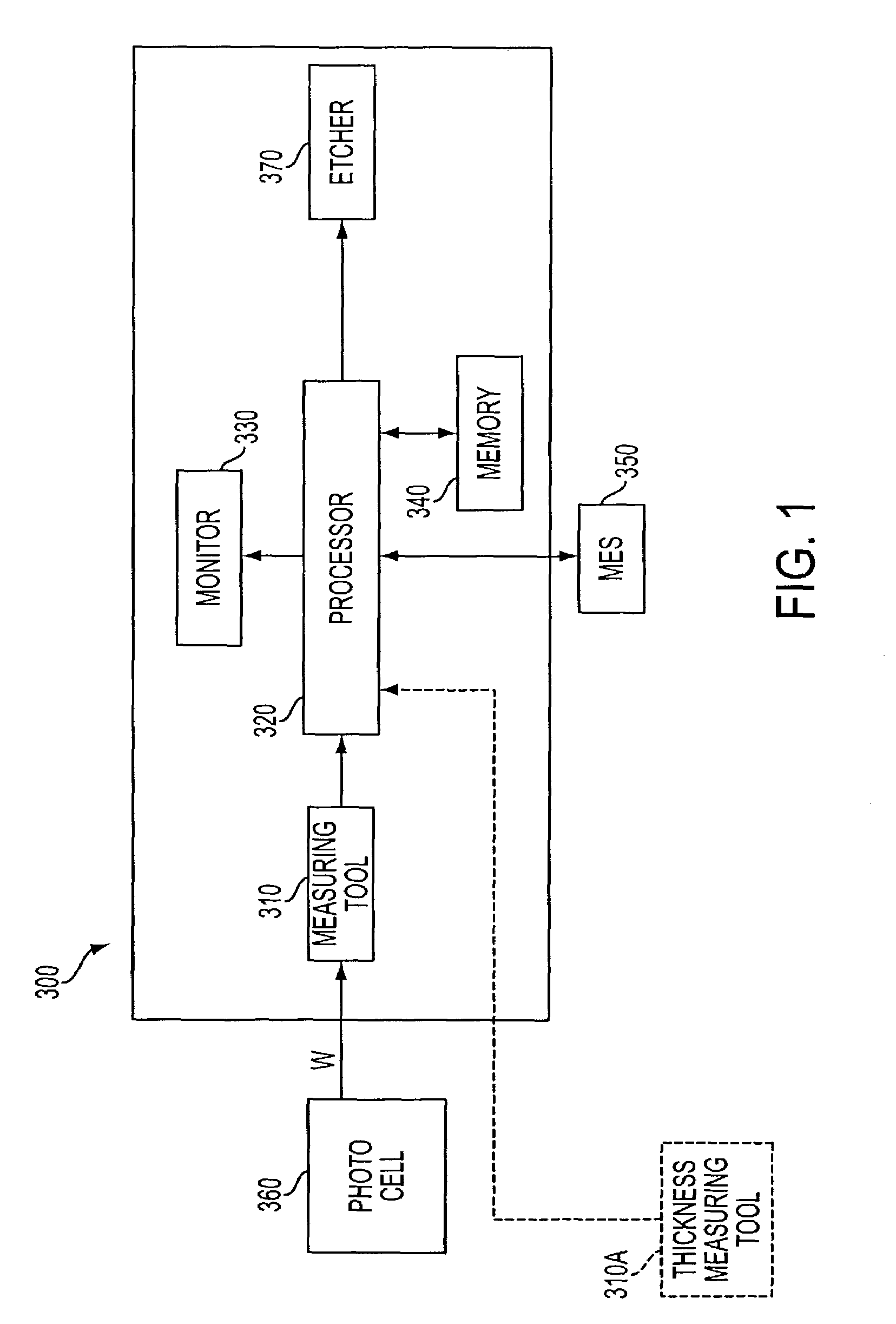
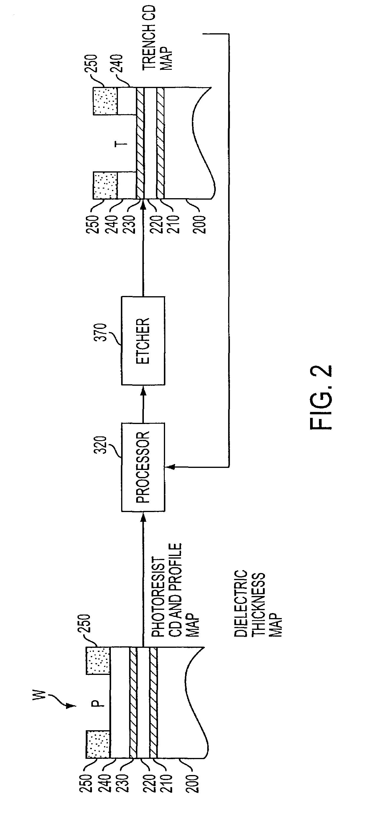
[0027]Conventional methodologies for in-process inspection of features formed on the surface of semiconductor wafers are not capable of analyzing CD and / or profile deviations from design rules in sufficient detail to provide information leading to early positive identification of the source of the defect or enabling process control to reduce dimensional variation. The present invention addresses the problem of CD control by reducing the CD variation by feeding forward information relating to photoresist mask CD and profile, and underlying layer thickness measured at several points on the wafer to adjust the next process the inspected wafer will undergo (e.g., the etch process). In certain embodiments of the present invention, the CD, profile and thickness measurement, etch processing and post-etch cleaning are performed at a single module in a controlled environment, thereby increasing throughput and improving yield. Thus, the present invention provides a self-contained etch module ...


PUM

PropertyMeasurementUnit
diameteraaaaaaaaaa
thicknessaaaaaaaaaa
dimensionaaaaaaaaaa

Abstract

A method and apparatus for processing a semiconductor wafer is provided for reducing dimensional variation by feeding forward information relating to photoresist mask CD and profile and underlying layer thickness measured at several points on the wafer to adjust the next process the inspected wafer will undergo (e.g., the etch process). After the processing step, dimensions of a structure formed by the process, such as the CD and depth of a trench formed by the process, are measured at several points on the wafer, and this information is fed back to the process tool to adjust the process for the next wafer to further reduce dimensional variation. In certain embodiments, the CD, profile, thickness and depth measurements, etch processing and post-etch cleaning are performed at a single module in a controlled environment. All of the transfer and processing steps performed by the module are performed in a clean environment, thereby increasing yield by avoiding exposing the wafer to the atmosphere and possible contamination between steps.

Description

FIELD OF THE INVENTION[0001]The present invention relates to a method and apparatus for monitoring and controlling processing carried out on a semiconductor substrate, and more particularly for controlling the uniformity of critical dimensions (CDs) and profiles of features formed on the semiconductor substrate through feedback and feed-forward of information gathered during in-process inspection of the features. The invention has particular applicability for in-line inspection of semiconductor wafers during manufacture of high-density semiconductor devices with submicron design features.BACKGROUND ART[0002]Current demands for high density and performance associated with ultra large scale integration require submicron features, increased transistor and circuit speeds and improved reliability. Such demands require formation of device features with high precision and uniformity, which in turn necessitates careful process monitoring, including frequent and detailed inspections of the d...

Claims


Application Information

Patent Timeline
Patent Type & Authority Patents(United States)
IPC IPC(8): H01L23/58G01N23/00H01L21/66
CPCH01L22/20H01L2924/0002H01L2924/00H01L22/00
Inventor LYMBEROPOULOS, DIMITRISHSUEH, GARYMOHAN, SUKESH
Owner APPLIED MATERIALS INC
Why Eureka
Try Eureka