Photovoltaic device and manufacturing method thereof

a photovoltaic device and manufacturing method technology, applied in the field of improved photovoltaic devices, can solve the problems of limited photovoltaic semiconductor layers, low conversion efficiency of solar cells for converting optical energy into electrical energy, and increase in material costs, so as to prevent a reduction in photoelectric conversion efficiency, increase in cost, and uneven

Inactive Publication Date: 2005-05-26
CANON KK
View PDF48 Cites 98 Cited by
  • Summary
  • Abstract
  • Description
  • Claims
  • Application Information

AI Technical Summary

Benefits of technology

[0014] An object of the present invention is to provide a structure of a photovoltaic device that prevents a reduction in photoelectric conversion efficiency due to the absence of preferable unevenness, an increase in cost due to the use of an expensive material, and a reduction in throughput in the conventional photovoltaic device, includes a power generating layer made from a thin film, which is formed in advance on a low cost substrate having preferable unevenness, and has a preferable characteristic and high productivity, and a method of manufacturing the photovoltaic device having the structure.

Problems solved by technology

Under the current circumstances, conversion efficiency of the solar cell for converting optical energy into electrical energy is low.
In addition, because a photovoltaic semiconductor layer requires a crystalline structure to obtain orientation, the photovoltaic semiconductor layer is limited to a polycrystalline silicon layer.
With respect to a manufacturing limitation, the base electroconductive layer and the polycrystalline silicon layer are formed at a temperature equal to or higher than 500° C. Therefore, it is necessary to use an expensive substrate made of, for example, glass resistant to such a high temperature.
Therefore, an increase in material cost and a reduction in throughput occur.
The uneven shape is technically achieved by controlling a size of a crystal grain and crystalline orientation, so that there is a limitation on an uneven difference of unevenness and a pitch thereof.
Accordingly, it is hard to obtain a large uneven difference and a large pitch.
However, the semiconductor thin film is not accurately formed on the base electroconductive layer along the base shape thereof, so that the unevenness on the surface of the semiconductor thin film tends to become dull.
Thus, with respect to the light incident side, it is not possible to sufficiently effectively use light with the unevenness.

Method used


Image

  • Photovoltaic device and manufacturing method thereof
  • Photovoltaic device and manufacturing method thereof
  • Photovoltaic device and manufacturing method thereof

Examples


embodiment 1

(Embodiment 1)

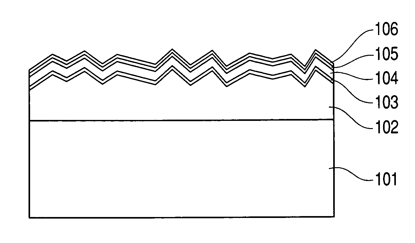
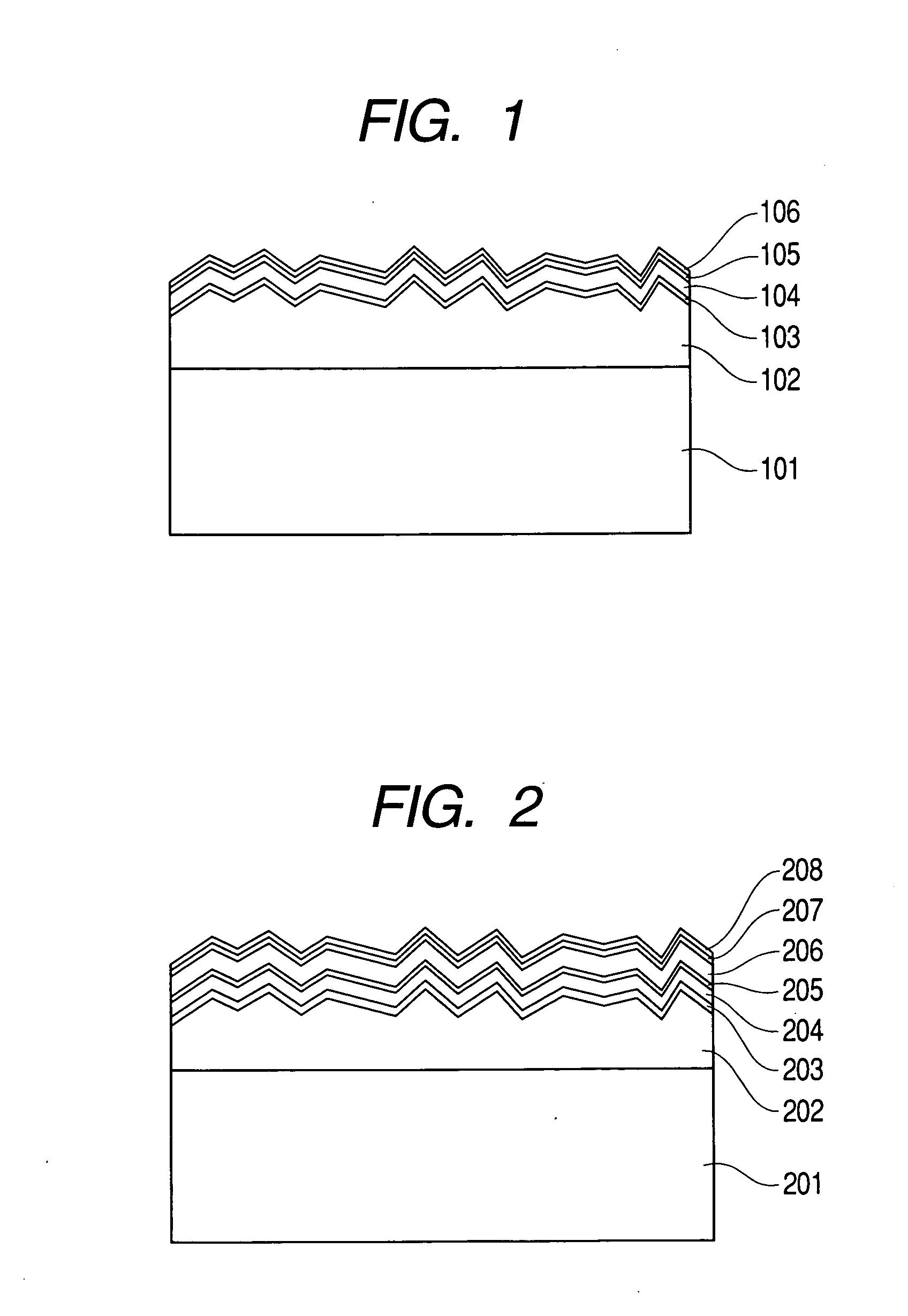
[0056]FIGS. 1 and 2 show the first example of the preferred embodiments of the present invention.

[0057]FIG. 1 shows a structure in which a polycrystalline silicon layer is formed on a silicon base by liquid phase growth to obtain a substrate and a single cell made of thin film system silicon is formed above the substrate.

[0058] In FIG. 1, a photovoltaic device includes a base 101 made of silicon, a polycrystalline silicon layer 102, an n-layer 103, an i-layer 104, a p-layer 105, and a transparent electrode layer 106. In such a structure, the base 101 and polycrystalline silicon layer 102 each have a p+ conductivity type. The n-layer 103 made of amorphous silicon (hereinafter referred to as a-Si), the i-layer 104 made of a-Si, amorphous silicon germanium (hereinafter referred to as a-SiGe), or micro-crystalline silicon (hereinafter referred to as μc-Si), and the p-layer 105 made of μc-Si are formed, and the transparent electrode layer 106 made of ITO or the like is fi...

embodiment 2

(Embodiment 2)

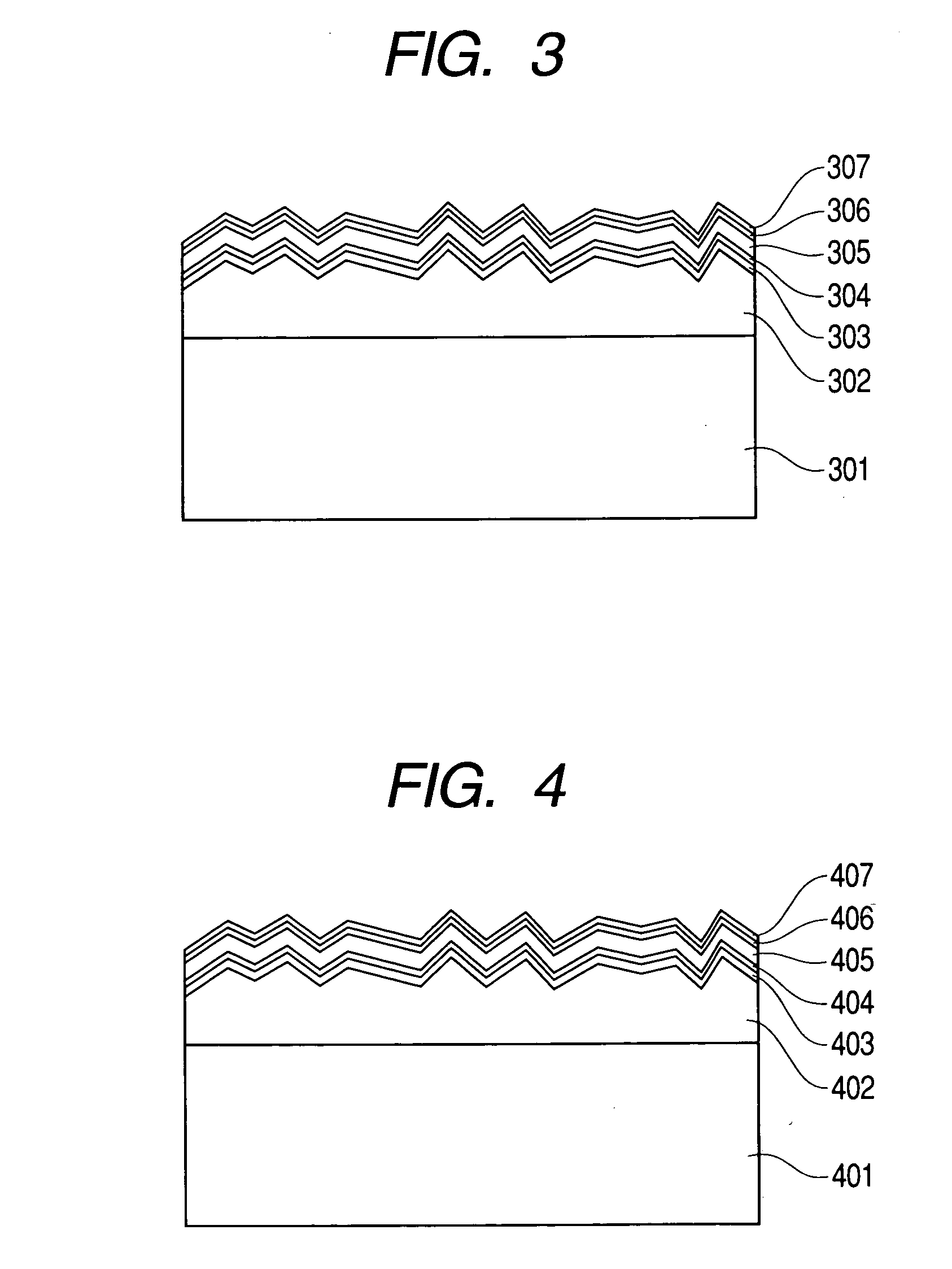
[0096]FIGS. 3 and 4 each show a double cell in Embodiment 2. According to a structure shown in FIG. 3, an emitter layer 303 is formed on a polycrystalline silicon layer 302 located on a base 301 to compose a polycrystalline pn-junction. A pin-junction composed of an n-layer 304, an i-layer 305, and a p-layer 306 is produced on the emitter layer 303. As a result, a photovoltaic device of a double cell is obtained as the entire structure. Reference numeral 307 denotes a transparent electrode layer. In such a structure, the base 301 has a conductivity type of n+, the polycrystalline silicon layer 302 has a conductivity type of n−, and the emitter layer 303 has a conductivity type of p+. The polycrystalline silicon layer 302 and the emitter layer 303 form the pn-junction and serve for a bottom cell. The n-layer 304, the i-layer 305, and the p-layer 306 form the pin-junction and serve for a top cell. Therefore, the photovoltaic device of the double cell is obtained as the e...

example 1

[0121] In this example, the solar cell having the single cell structure shown in FIG. 2 was manufactured.

[0122] First, an ingot was produced using a nugget of chemical grade metallurgical grade silicon from Norway as a raw material. After 60 kg of the nugget was cleaned with acid, the nugget was placed in the apparatus shown in FIG. 17. In the crucible 1703, a bottom surface is 30 cm square and a depth is 40 cm. The heater 1702 was controlled and the entire silicon was melted for 10 hours to degas. After that, slow cooling was performed by the cooling plate 1701, so that the silicon was solidified from the bottom surface of the crucible 1703 as shown in FIG. 17. Reference numeral 1704 denotes the solidified silicon and 1705 denotes the melted silicon. The solidification was completed after 10 hours. Then, cooling was performed for 10 hours while the output of the heater 1702 was gradually reduced. Grain boundaries was extended in the longitudinal direction in the ingot produced by ...


PUM

PropertyMeasurementUnit
tilt anglesaaaaaaaaaa
resistivityaaaaaaaaaa
lengthaaaaaaaaaa

Abstract

There is provided a photovoltaic device in which at least one pin-junction is formed in a thin film semiconductor deposited on a substrate, the substrate including: a base including polycrystalline silicon; and a polycrystalline silicon layer formed on the base by liquid phase growth, in which at least a part of a surface of the polycrystalline silicon layer has unevenness composed of facet surfaces. The photovoltaic device prevents a reduction in photoelectric conversion efficiency due to the absence of preferable unevenness, an increase in cost due to the use of an expensive material, and a reduction in throughput in the photovoltaic device, and has a preferable characteristic and high productivity.

Description

BACKGROUND OF THE INVENTION [0001] 1. Field of the Invention [0002] The present invention relates to an improved photovoltaic device, more particularly to a structure for effectively utilizing incident light on a photovoltaic device and a method of manufacturing a photovoltaic device having the structure. [0003] 2. Related Background Art [0004] A solar cell which is an application example of a photovoltaic device using a semiconductor has received attention as a device for solving energy problems and environmental problems. In recent years, practical use of the solar cell has been promoted to such an extent that the solar cell mounted on a roof of a general house may cover power consumption of the house. Such a solar cell is mainly made of a semiconductor such as silicon or CdS. In particular, because of pollution free and a large amount of deposits, silicon is the most widespread material for the solar cell under the current circumstances. [0005] The silicon used for manufacturing ...

Claims


Application Information

Patent Timeline
Patent Type & Authority Applications(United States)
IPC IPC(8): H01L31/00H01L31/0236H01L31/0368H01L31/04H01L31/075H01L31/077H01L31/18
CPCH01L31/03682H01L31/077H01L31/02363Y02B10/12Y02E10/546H01L31/182Y02B10/10Y02E10/548Y02P70/50
Inventor MURAKAMI, TSUTOMUNISHIDA, SHOJI
Owner CANON KK
Why Eureka
Try Eureka