Charged particle beam exposure apparatus and method of manufacturing semiconductor device

a technology of charged particle beam and exposure apparatus, which is applied in the direction of electrical apparatus, irradiation devices, electric discharge tubes, etc., can solve the problems of inability to achieve practical processing speed and difficulty in forming patterns having a line width of 20 nm or less, so as to reduce the time required for exposure, the effect of increasing the proportion of charged particle beams actually used for exposure to all of the charged particle beams and improving the usage efficiency of charged particle beams generated from th

Active Publication Date: 2015-08-27
ADVANTEST CORP
View PDF10 Cites 119 Cited by
  • Summary
  • Abstract
  • Description
  • Claims
  • Application Information

AI Technical Summary

Benefits of technology

[0017]According to the aspects described above, the irradiation of the plurality of charged particle beams arranged in the direction orthogonal to the line patterns is performed while moving the one-dimensional array beam formed of the plurality of charged particle beams in the direction parallel to the line pattern. Since the one-dimensional array beam is used as described above, the proportion of the charged particle beams actually used for the exposure to all of the charged particle beams can be increased. The usage efficiency of the charged particle beams generated from the charged particle source is thus improved and the time required for the exposure can be reduced.
[0018]Moreover, performing the irradiation of the charged particle beams while stopping the one-dimensional array beam for a certain period at pixel positions set at regular intervals on the line patterns in accordance with the movement of the stage can make rising of exposure amount distribution steep. The cut patterns and via patterns can be thereby drawn in high resolution and in high accuracy.

Problems solved by technology

Since the wavelength of this light is long, formation of a pattern having a line width of 20 nm or less is difficult even when various techniques for improving resolution are used.
However, this technique has the following problem.
Since it is difficult to obtain a charged particle beam of a sufficient intensity while maintaining high resolution, a practical processing speed cannot be obtained when a fine circuit pattern of a semiconductor device in which an area of a portion to be exposed is large is directly drawn only by using the charged particle beam.

Method used


Image

  • Charged particle beam exposure apparatus and method of manufacturing semiconductor device
  • Charged particle beam exposure apparatus and method of manufacturing semiconductor device
  • Charged particle beam exposure apparatus and method of manufacturing semiconductor device

Examples


first embodiment

[0049](1) Configuration of Electron Beam Exposure Apparatus

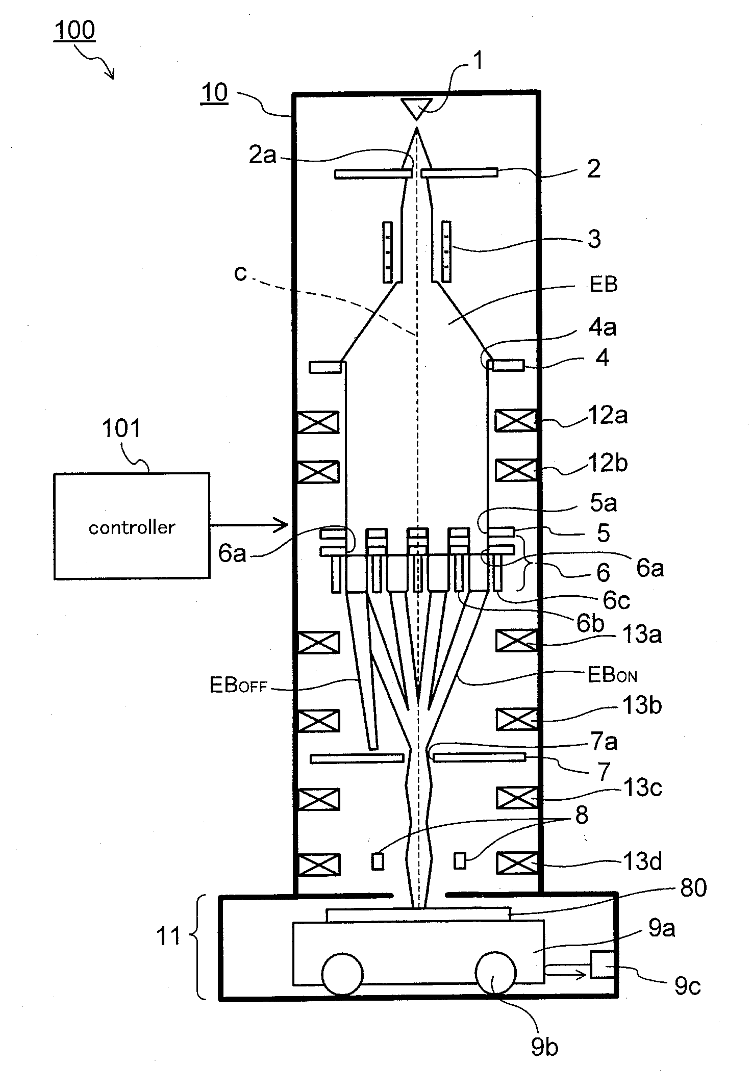
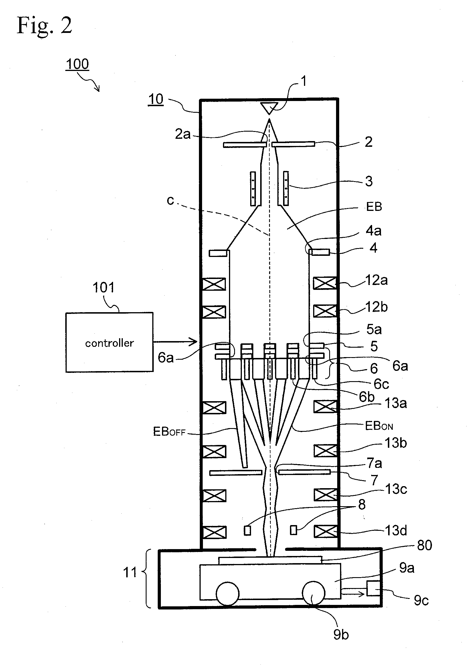
[0050]FIG. 2 is a cross-sectional view of one column in an electron beam exposure apparatus of the embodiment.

[0051]The electron beam exposure apparatus 100 of the embodiment irradiates a surface of a semiconductor substrate 80 being an exposure target with electron beam EB (charged particle beam) by using the column 10 shown in FIG. 2. The column 10 includes a cylindrical case, and an electron gun 1 configured to generate the electron beam EB is provided inside the case near an upper end thereof.

[0052]The electron beam EB is emitted from the electron gun 1 at a predetermined accelerating voltage (for example, 50 keV), and is shaped to have a circular cross section about an optical axis c by passing through an opening 2a of a first aperture plate 2.

[0053]The electron beam EB having passed through the first aperture plate 2 passes through an asymmetric illumination optical system 3 provided below the first aperture plate 2. T...

second embodiment

[0163]The first embodiment shows an example in which the exposure amounts Dp and Dp+1 are linear functions of the internal ratio r. However, the present invention is not limited to this example.

[0164]In the embodiment, description is given of an example in which the exposure amounts Dp and Dp+1 are polynomials of the internal ratio r to further improve the accuracy.

[0165]As described with reference to FIG. 9, when the exposure amounts Dp and Dp+1 are linear functions of the internal ratio r, there is a variation of even function about the position of r=0.5 in the line width.

[0166]In view of this, in the embodiment, the variation of the line width of the cut pattern is further reduced as follows. For example, a fourth-order term and a sixth-order term are added as higher-order terms to cancel out an even function term appearing in the variation of the line width of FIG. 9 (curved line 99a).

[0167]Moreover, regarding the displacement of the cut pattern, for example, a third-order term ...

third embodiment

[0172]FIG. 14 is a perspective view showing a main portion of an electron beam exposure apparatus of a third embodiment.

[0173]As shown in FIG. 14, in the embodiment, a plurality of the columns 10 are arranged above the stage 9a. The structure of each of the columns 10 is the same as that of the column 10 shown in FIG. 3. Each column 10 can be formed to have a diameter of about 30 mm for example.

[0174]FIG. 15 is a plan view showing regions in which the respective columns 10 perform exposure when the columns each having a diameter of 30 mm are arranged on a semiconductor substrate having a diameter of 300 mm.

[0175]As shown in FIG. 15, 88 columns 10 can be arranged on the semiconductor substrate 80 having the diameter of 300 mm, and each of the columns 10 performs exposure on a region of 30 mm×30 mm. In the embodiment, since the plurality of columns 10 can perform exposure in parallel with each other, the exposure of cut patterns or via patterns can be more quickly performed.

[0176]A de...


PUM


Abstract

The invention relates to a charged particle beam exposure apparatus configured to expose cut patterns or via patterns on a substrate having a plurality of line patterns 81a arranged on an upper surface of the substrate at a constant pitch by irradiating the substrate with a plurality of charged particle beams B1 to Bn while moving a one-dimensional array beam A1 in an X direction parallel to the line patterns 81a, the one-dimensional array beam A1 being a beam in which the charged particle beams B1 to Bn are arranged in an Y direction orthogonal to the line patterns 81a.

Description

CROSS REFERENCE TO RELATED APPLICATIONS [0001]This application is based upon and claims the benefit of priority of the prior Japanese Patent Application No. 2014-035755, filed on Feb. 26, 2014, the entire contents of which are incorporated herein by reference.TECHNICAL FIELD [0002]The embodiments discussed herein are related to a charged particle beam exposure apparatus and a method of manufacturing a semiconductor device by using the same.BACKGROUND ART [0003]Along with progress of higher integration of semiconductor devices, there is a demand for an exposure technique which can form finer patterns and a new exposure technique is being developed. Currently, in an optical exposure technique used for manufacturing of state-of-the-art semiconductor devices, light from an ArF light source is used. Since the wavelength of this light is long, formation of a pattern having a line width of 20 nm or less is difficult even when various techniques for improving resolution are used.[0004]An...

Claims


Application Information

Patent Timeline
Patent Type & Authority Applications(United States)
IPC IPC(8): H01J37/317H01J37/20H01L21/268H01J37/30
CPCH01J37/3174H01J37/3007H01J37/20H01J2237/303H01J2237/202H01J2237/1502H01J2237/31728H01L21/268H01J37/3045G21K5/10H01J2237/0435
Inventor YAMADA, AKIO
Owner ADVANTEST CORP
Why Eureka
Try Eureka