Batch processing method for forming structure including amorphous carbon film

Active Publication Date: 2010-12-09
TOKYO ELECTRON LTD
View PDF4 Cites 23 Cited by
  • Summary
  • Abstract
  • Description
  • Claims
  • Application Information

AI Technical Summary

Benefits of technology

[0008]An object of the present invention is to provide a batch processing method f

Problems solved by technology

Accordingly, it has become difficult to ensure a sufficient etching resistance only by a photo-resist film.
In general, where plasma CVD apparatuses of the single-substrate type are used to form a thin film, the coverage performance of the f

Method used


Image

  • Batch processing method for forming structure including amorphous carbon film
  • Batch processing method for forming structure including amorphous carbon film
  • Batch processing method for forming structure including amorphous carbon film

Examples


Example

First Embodiment

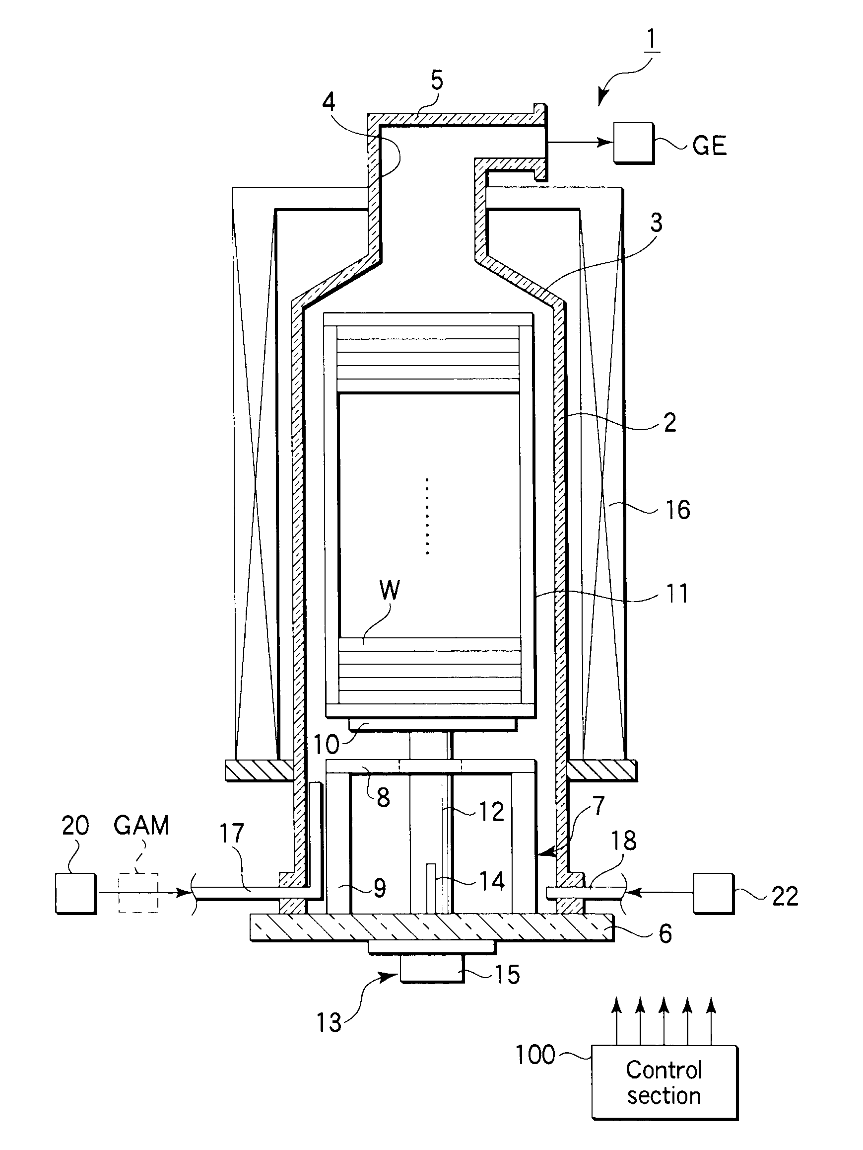
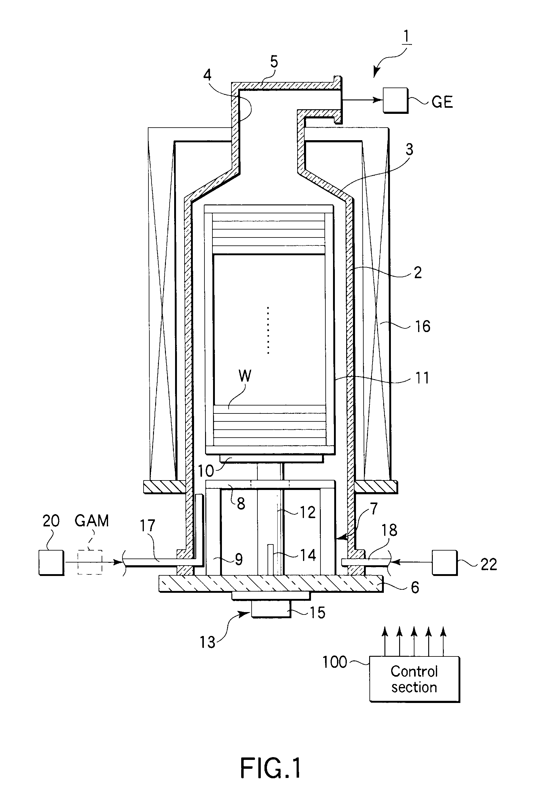
[0059]FIG. 3 is a view showing the recipe of a batch processing method for forming a structure including an amorphous carbon film according to a first embodiment of the present invention. In this method, an N2 preliminary treatment (high-temperature N2 purge) is first performed to remove water (moisture) from the surface of the underlying layer on each of the semiconductor wafers W. Then, an amorphous carbon film is formed on the underlying layer.

[0060]Specifically, at first, the inside of the reaction tube 2 is heated by the heater 16 at a predetermined load temperature, such as 300° C., as shown in FIG. 3, (a). Further, nitrogen (N2) gas is supplied through the purge gas feed line 18 into the reaction tube 2 at a predetermined flow rate, such as 1 slm (1 liter / min), as shown in FIG. 3, (c). Then, a wafer boat 11 that holds semiconductor wafers W is placed on the lid 6, and the lid 6 is moved up by the boat elevator 128. Consequently, the wafer boat 11 with the semi...

Example

Second Embodiment

[0074]FIG. 6 is a view showing the recipe of a batch processing method for forming a structure including an amorphous carbon film according to a second embodiment of the present invention. In this method, an ammonia preliminary treatment (high-temperature ammonia purge) is first performed to remove water (moisture) from the surface of the underlying layer on each of the semiconductor wafers W. Then, an amorphous carbon film is formed on the underlying layer.

[0075]Specifically, at first, the inside of the reaction tube 2 is heated by the heater 16 at a predetermined load temperature, such as 300° C., as shown in FIG. 6, (a). Further, nitrogen (N2) gas is supplied through the purge gas feed line 18 into the reaction tube 2 at a predetermined flow rate, such as 1 slm (1 liter / min), as shown in FIG. 6, (c). Then, a wafer boat 11 that holds semiconductor wafers W is placed on the lid 6, and the lid 6 is moved up by the boat elevator 128. Consequently, the wafer boat 11 w...

Example

Third Embodiment

[0092]FIG. 10 is a view showing the recipe of a batch processing method for forming a structure including an amorphous carbon film according to a third embodiment of the present invention. In this method, a preliminary treatment is performed to form a hydrophobic layer consisting of silicon by CVD, while supplying BTBAS (bistertialbutylaminosilane) gas, to cover the underlying layer on each of the semiconductor wafers W with the hydrophobic layer. Then, an amorphous carbon film is formed on the hydrophobic layer.

[0093]Specifically, at first, the inside of the reaction tube 2 is heated by the heater 16 at a predetermined load temperature, such as 300° C., as shown in FIG. 10, (a). Further, nitrogen (N2) gas is supplied through the purge gas feed line 18 into the reaction tube 2 at a predetermined flow rate, such as 1 slm, as shown in FIG. 10, (c). Then, a wafer boat 11 that holds semiconductor wafers W is placed on the lid 6, and the lid 6 is moved up by the boat elev...


PUM

PropertyMeasurementUnit
Temperatureaaaaaaaaaa

Abstract

A batch processing method for forming a structure including an amorphous carbon film includes performing a preliminary treatment of removing water from a surface of the underlying layer by heating the inside of the reaction chamber at a preliminary treatment temperature of 800 to 950° C. and supplying a preliminary treatment gas selected from the group consisting of nitrogen gas and ammonia gas into the reaction chamber while exhausting gas from inside the reaction chamber; and, then performing main CVD of forming an amorphous carbon film on the underlying layer by heating the inside of the reaction chamber at a main process temperature and supplying a hydrocarbon gas into the reaction chamber while exhausting gas from inside the reaction chamber.

Description

CROSS-REFERENCE TO RELATED PATENT APPLICATIONS[0001]This application claims the benefit of priority from Japanese Patent Applications No. 2009-135483, filed on Jun. 4, 2009, and No. 2010-094417, filed on Apr. 15, 2010, in the Japan Patent Office, the disclosure of both of which is incorporated herein in the entirety by reference.BACKGROUND OF THE INVENTION[0002]1. Field of the Invention[0003]The present invention relates to a batch processing method for forming a structure including an amorphous carbon film on target objects, such as semiconductor wafers, in a semiconductor process. The term “semiconductor process” used herein includes various kinds of processes which are performed to manufacture a semiconductor device or a structure having wiring layers, electrodes, and the like to be connected to a semiconductor device, on a target object, such as a semiconductor wafer or a glass substrate used for an FPD (Flat Panel Display), e.g., an LCD (Liquid Crystal Display), by forming semi...

Claims


Application Information

Patent Timeline
IPC IPC(8): H01L21/3205G05B21/00
CPCC23C16/0209C23C16/0272C23C16/26H01L21/3146H01L21/02271H01L21/02304H01L21/02312H01L21/02115H01L21/02592H01L21/324
Inventor OKADA, MITSUHIROTOJO, YUKIO
Owner TOKYO ELECTRON LTD
Why Eureka
Try Eureka