Semiconductor device with silicon-germanium gate electrode and method for manufacturing thereof

Inactive Publication Date: 2005-03-03
SHARP KK
View PDF8 Cites 19 Cited by
  • Summary
  • Abstract
  • Description
  • Claims
  • Application Information

AI Technical Summary

Benefits of technology

[0018] A more specific object of the present invention is to form a void-free SiGe film having good surface flatness on a high-k film. Another

Problems solved by technology

However, in case of that the thin SiO2 film is used as the gate dielectric film, gate current leakage owing to tunnel current leakage cannot be ignore as compared with source-drain current, thereby arising problems in the highly integration and power saving of MOSFETs.
However, in this case, there is a problem of the occurrence of silicide cohesion and defective resistance caused by Ge in the SiGe film.
Also, there are problems that a surface of a SiGe film is roughened during formation of the SiGe film and it is difficult of patterning agate electrode using dry etching.
However, according to investigation by the present inventors, when a cap Si film is formed on the SiGe film, there are problems su

Method used


Image

  • Semiconductor device with silicon-germanium gate electrode and method for manufacturing thereof
  • Semiconductor device with silicon-germanium gate electrode and method for manufacturing thereof
  • Semiconductor device with silicon-germanium gate electrode and method for manufacturing thereof

Examples


Example

[0037] First Embodiment

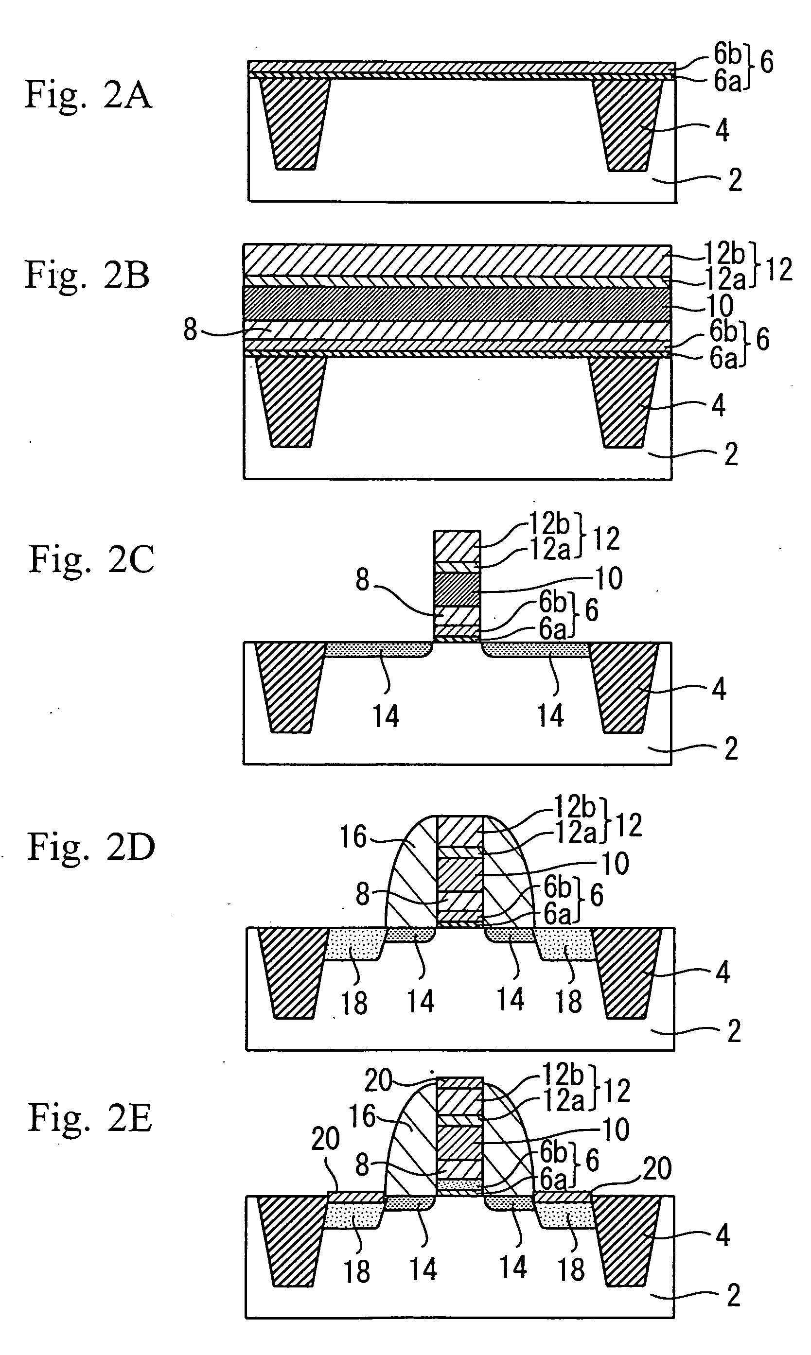
[0038] First, the structure of a semiconductor device according to a first embodiment of the present invention will be described.

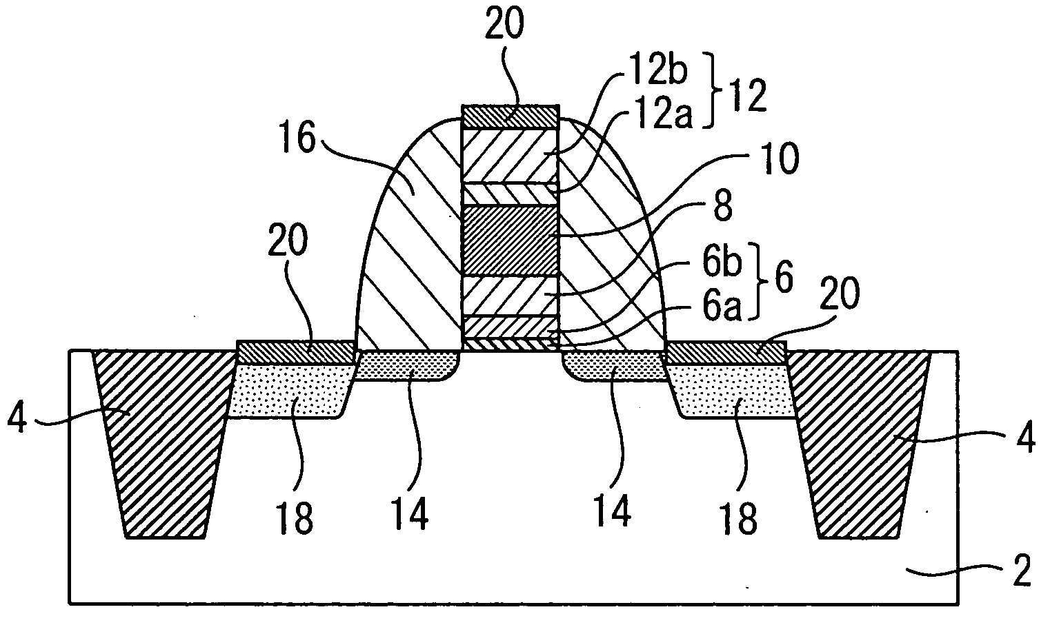
[0039]FIG. 1 is a schematic cross-sectional view for illustrating a semiconductor device according to a first embodiment of the present invention.

[0040] As FIG. 1 shows, a silicon substrate serving as the substrate 2 has element regions on which semiconductor elements such as transistors are formed, and isolation regions for isolating the element regions, in which field insulating films (also referred to as “element-isolating insulating films”) 4 are formed. Well regions (not shown) are formed in the element regions of the substrate 2.

[0041] On the substrate 2 in the element regions, a gate dielectric film 6 is formed. The gate dielectric film 6 is laminated film includes: an underlying interfacial layer 6a formed on the silicon substrate 2; and high-k dielectric film 6b formed on the underlying interfacial layer 6a and having hi...

Example

[0086]FIG. 5 is a schematic cross-sectional view for illustrating a semiconductor device according to a second embodiment of the present invention.

[0087] The semiconductor device according to the second embodiment shown in FIG. 5 differs from the above-described semiconductor device according to the first embodiment in that the upper cap Si film 12b and the silicide layers 20 are not formed. Other structure is the same as the first embodiment.

[0088] Next, a method for manufacturing the semiconductor device will be described.

[0089]FIGS. 6A to 6D are process sectional views for illustrating a method for manufacturing the semiconductor device according to the second embodiment.

[0090] First, in the same manner as in the manufacturing method according to the first embodiment, elements up to the high-k dielectric film 6b are formed. Thus, the structure shown in FIG. 6A is attained.

[0091] As described in the first embodiment, after formation of the high-k dielectric film 6b, thermal p...

Example

[0098] Third Embodiment

[0099]FIG. 7 is a schematic cross-sectional view for illustrating a semiconductor device according to a third embodiment of the present invention. Specifically, FIG. 7 is a schematic cross-sectional view for illustrating a CMOS (complementary metal oxide semiconductor) application.

[0100] As FIG. 7 shows, field insulating films 22 are formed in a silicon substrate 21. NMOS (n-channel MOS) regions and PMOS (p-channel MOS) regions are isolated by the field insulating films 22. P-well regions 23 are formed in the silicon substrate 21 of the NMOS regions, and n-well regions 24 are formed in the silicon substrate 21 of the PMOS regions.

[0101] On the p-well regions 23 and n-well regions 24, a gate dielectric film 25 laminated an underlying interfacial layer 25a and a high-k dielectric film 25b is formed in the same way as the first embodiment.

[0102] On the gate dielectric film 25 is formed a gate electrode composed of the laminate of a seed Si film 26, a SiGe fil...


PUM


Abstract

A semiconductor includes a gate electrode having a SiGe film on a a gate dielectric film that is on a silicon substrate. The gate dielectric film includes an underlying interfacial layer on the substrate, and a high-k dielectric film having higher dielectric constant than the underlying interfacial layer. The gate electrode includes a seed Si film on the high-k dielectric film and a SiGe film formed on the seed Si film. The seed Si film has a thickness of 0.1 nm or more and smaller than 5 nm.

Description

[0001] 1. Field of the Invention [0002] The present invention relates to a semiconductor device and to a method for manufacturing thereof. More specifically the present invention relates to a gate electrode including a thin SiGe film and to a method for manufacturing thereof. [0003] 2. Description of the Background Art [0004] In recent years, MOSFET (metal oxide semiconductor field effect transistor) as a semiconductor device has been extremely miniaturized and highly integrated. Concurrent to this trend, the thickness of a gate dielectric film has been reduced from the point of view of securing the driving current and saving power consumption. For meet the demands of scaling lows, the thickness of a silicon oxide film (SiO2 film) which has been used as a gate dielectric film, need to be 2 nm or less. [0005] However, in case of that the thin SiO2 film is used as the gate dielectric film, gate current leakage owing to tunnel current leakage cannot be ignore as compared with source-dr...

Claims


Application Information

Patent Timeline
IPC IPC(8): H01L21/28H01L29/423H01L21/314H01L21/336H01L21/8238H01L29/49H01L29/51H01L29/78
CPCH01L21/28044H01L29/7833H01L21/28194H01L21/28202H01L21/28211H01L21/3141H01L21/823828H01L21/823835H01L21/823857H01L29/4925H01L29/513H01L29/517H01L29/518H01L29/665H01L21/28185H01L21/02181H01L21/02178H01L21/02194H01L21/0228H01L21/28255
Inventor MUTOU, AKIYOSHIOHJI, HIROSHI
Owner SHARP KK
Why Eureka
Try Eureka