Interposer and semiconductor device employing same, and method for manufacturing semiconductor device

a technology of semiconductor devices and interposers, which is applied in the direction of semiconductor devices, semiconductor/solid-state device details, electrical devices, etc., can solve the problems of poor stiffness of the interposer, reduced device production yield, and inability to meet, so as to improve the production yield of the semiconductor device 100, improve the flatness of the surface, and reduce the effect of bending

Inactive Publication Date: 2006-10-12
RENESAS ELECTRONICS CORP
View PDF4 Cites 23 Cited by
  • Summary
  • Abstract
  • Description
  • Claims
  • Application Information

AI Technical Summary

Benefits of technology

[0079] Next, advantageous effects obtainable by employing the configuration of the present embodiment will be described.
[0080] In the present embodiment, a concave curvature is provided to the organic resin substrate 101 in the side of the device mounting surface 111 in advance. This is configured to previously provide the curving substrate so as to have an inverted aspect from the bending that will be spontaneously generated in the assembly process. Such organic resin substrate 101 is employed to assemble the package of the semiconductor device 100, and the bending generated in the assembly process causes a stretching of the organic resin substrate 101 that is deliberately bent in advance. Consequently, even if a bending is generated in the interposer 102 to convexly warp the device mounting surface 111 by heating thereof in the process for assembling the semiconductor device 100, and more specifically in the process operation of joining the semiconductor chip 105 and the process operation of forming the underfill resin layer 109, the bending spontaneously generated in the manufacturing process can be compensated with the bending deliberately provided to the organic resin substrate 101. Thus, the semiconductor device 100 after the completion of the manufacture can be configured to exhibit better flatness of the surface of the organic resin substrate 101, as compared with the conventional device. Since the organic resin substrate 101 is provided with the planarized surface after the assembly process as described above, a planarization on the order of a level for fully satisfying the required co-planarity of, for example, not larger than 150 μm or not larger than 200 μm can be achieved, even in the case of employing no lid, thereby providing an improved production yield of the semiconductor device 100.
[0081] Further, the conventional interposer may exhibit more considerable bending when the semiconductor chip 105 is joined thereto, since the conventional interposer may have a convex bending in the side of the device mounting surface 111, contrary to the interposer of the present embodiment. On the contrary, since the inverted curvature, which has the inverted aspect from the aspect of the spontaneous bending generated in the operation of joining the semiconductor chip 105 thereto, is previously provided to the surface of the organic resin substrate 101 according to the present embodiment, a reverse bending generated in the process of mounting the semiconductor chip 105 can be utilized to planarize the organic resin substrate 101 at the stage of the completion of the assembly of the device.
[0082] Such advantageous effect can be considerably exhibited, when the lead free solder having relatively higher stiffness is employed as the solder ball 107. In addition, such advantageous effect can also be considerably exhibited in the case of the semiconductor device 100 that is employed without adhering the lid after the process operation described above in reference to FIG. 7C. In addition, such advantageous effect can also be considerably exhibited when the organic resin substrate 101 has a reduced thickness. Even if the interposer can not have sufficient stiffness for withstanding the stress due to the bending thereof generated in the manufacturing process, such as in the case that, for example, sufficient thickness of the interposer can not be assured for the reason of ensuring the necessary electrical characteristics, the configuration according to the present embodiment provides better flatness of the organic resin substrate 101 after the assembly of the semiconductor device 100, and therefore the requirement in the co-planarity can be satisfied.
[0083] Further, in the present embodiment, the curvature is formed by disposing the back surface-side PET film 129 on the bottom of the organic resin substrate 101 and pressurizing these members from the upward. Consequently, a level of the curvature h of the organic resin substrate 101 can be easily adjusted by suitably selecting the thickness and the number of the PET film 135a to the PET film 135c composing the back surface-side PET film 129. Second Embodiment
[0084] While the curvature is formed by disposing the organic resin substrate 101 and the stiffener 103 between the PET films and evacuating and releasing the atmosphere in first embodiment, another procedure for creating a curvature may also be employed, in which an interposer and a stiffener may be aligned onto a jig having a concave portion corresponding to a level of the curvature h, and a punch having a convex portion that inversely follows the concave portion is lifted down from the upper direction to form a concave curvature in the side of the device mounting surface 111 while adhering the interposer with the stiffener. Descriptions of the exemplary implementation employing a metal mold will be made as follows.

Problems solved by technology

In addition, such interposer is made of a material having poor stiffness, as compared with silicon.
Consequently, sufficient stiffness of such interposer for withstanding a bending generated by factors such as a difference in thermal expansion coefficient between the semiconductor chip and the interposer, a shrinkage occurred in a cure of a liquid resin and the like, cannot be ensured, and therefore a side of a device mounting surface of the interposer is easily bent to form a convex shape after the completion of the assembly of the semiconductor package.
Further, specification in flatness after the assembly (co-planarity) cannot be satisfied, even if the technology described in the above-described in Japanese Patent Laid-Open No. 2000-323,624 is employed, and thus there is a concern that production yield of devices may be reduced.
H10-326,800 involves conducting a processing for bending the substrate after the semiconductor is mounted on the substrate, there is a concern that the semiconductor may be damaged in such processing.

Method used


Image

  • Interposer and semiconductor device employing same, and method for manufacturing semiconductor device
  • Interposer and semiconductor device employing same, and method for manufacturing semiconductor device
  • Interposer and semiconductor device employing same, and method for manufacturing semiconductor device

Examples


first embodiment

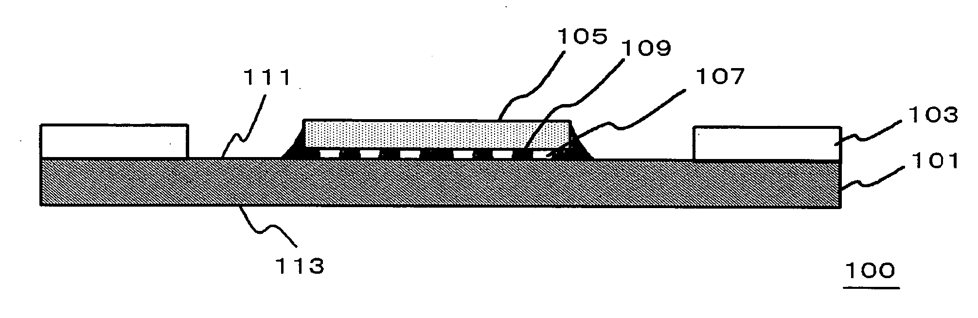
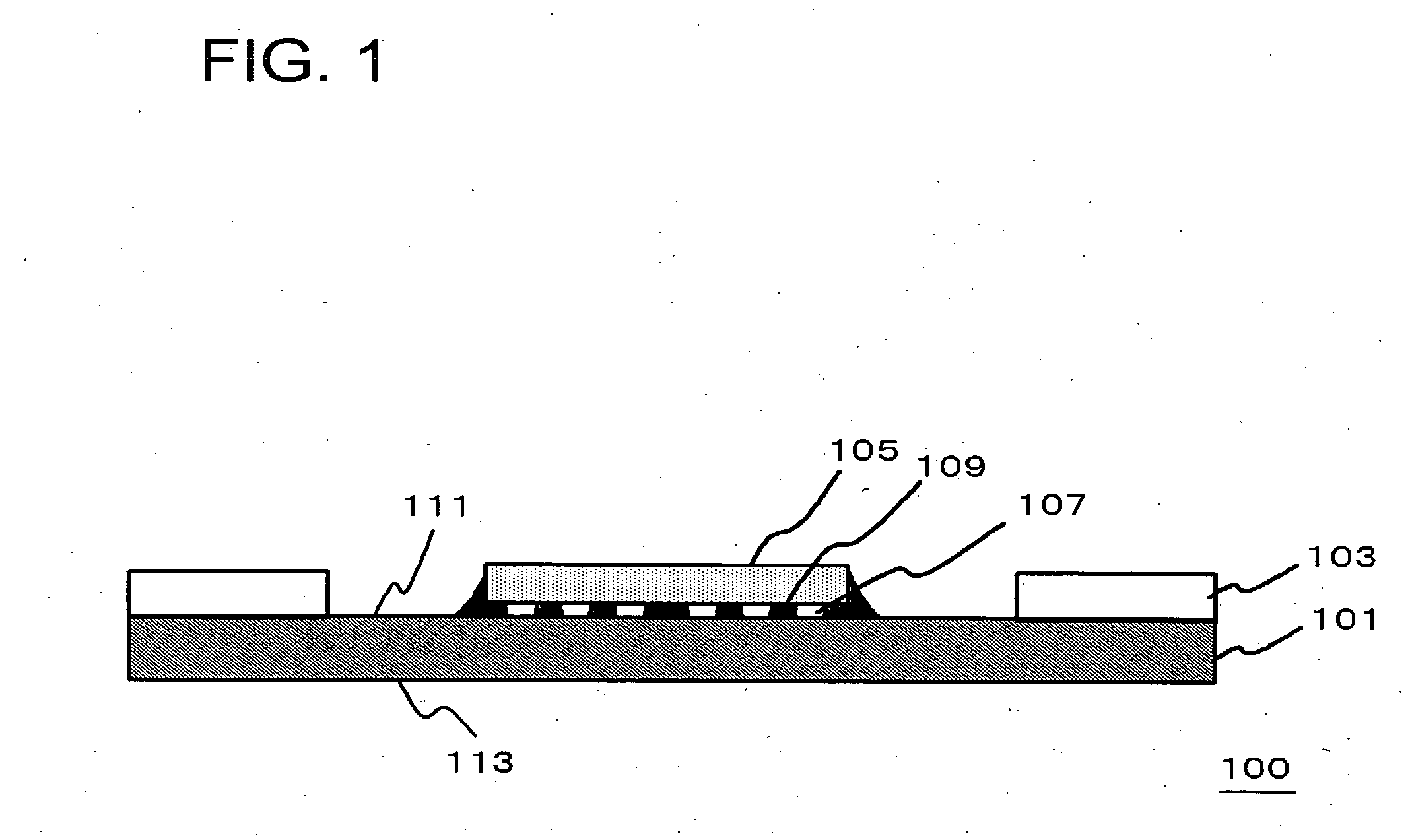
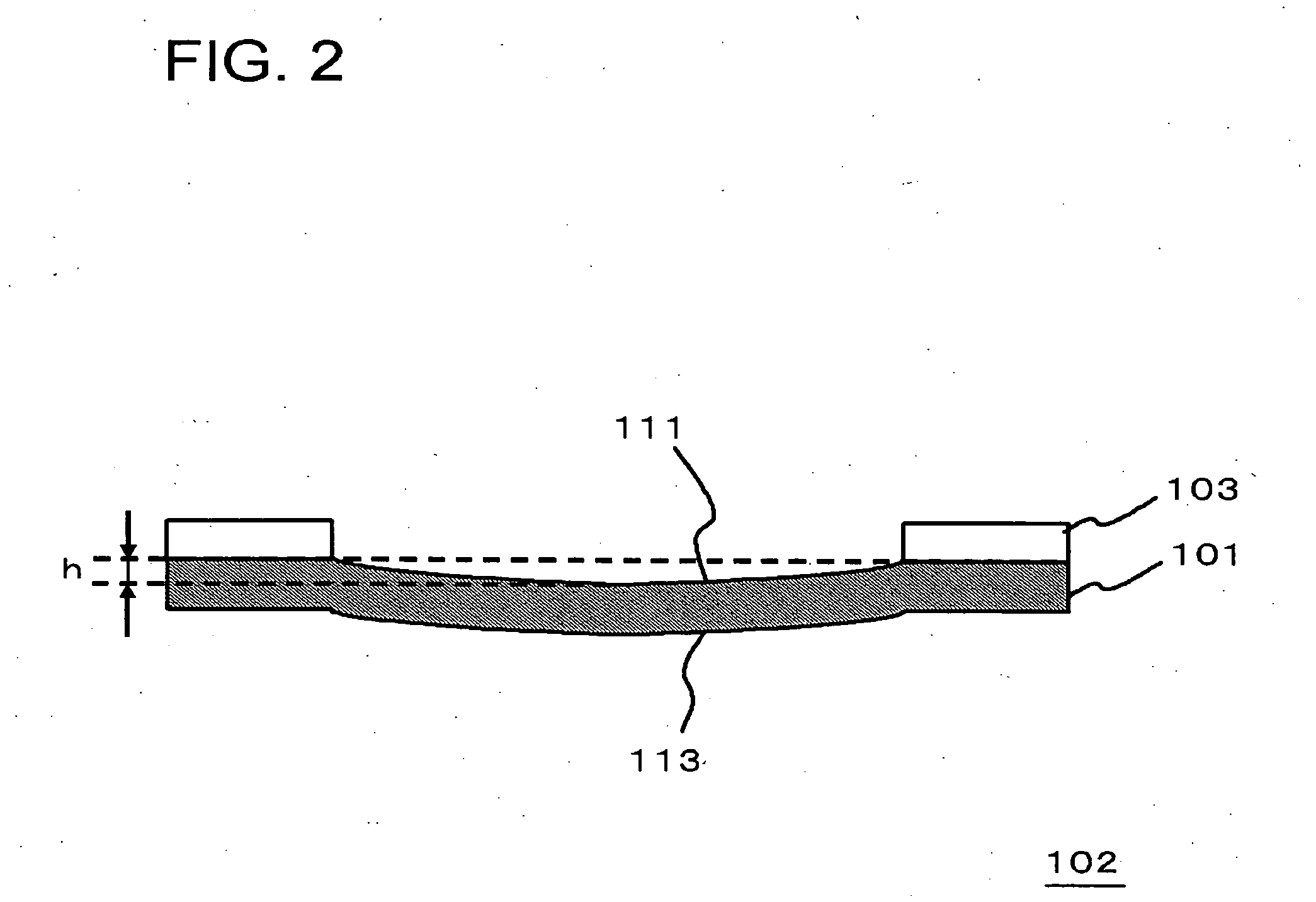
[0049]FIG. 2 is a cross-sectional view, illustrating a configuration of an interposer of the present embodiment. FIG. 1 is a cross-sectional view, illustrating a configuration of a semiconductor device produced by employing the interposer shown in FIG. 2. The interposer shown in FIG. 2 is an interposer, which is composed of an organic resin substrate 101, and on one surface of which a semiconductor device (semiconductor chip 105 shown in FIG. 1) is mounted, and has a convex curvature in a side of a back surface 113 opposite to the device mounting surface 111. A height of a highest point of the device mounting surface 111 from a flat plane is, for example, 10 μm or more and 150 μm or less, when an organic resin substrate 101 of the interposer is disposed on the flat plane so that the back surface 113 faces toward an upward direction. In addition, a stiffener 103 that surrounds the device mounting region is joined to the device mounting surface of the organic resin substrate 101 to fo...

second embodiment

[0084] While the curvature is formed by disposing the organic resin substrate 101 and the stiffener 103 between the PET films and evacuating and releasing the atmosphere in first embodiment, another procedure for creating a curvature may also be employed, in which an interposer and a stiffener may be aligned onto a jig having a concave portion corresponding to a level of the curvature h, and a punch having a convex portion that inversely follows the concave portion is lifted down from the upper direction to form a concave curvature in the side of the device mounting surface 111 while adhering the interposer with the stiffener. Descriptions of the exemplary implementation employing a metal mold will be made as follows.

[0085]FIG. 8 is a perspective view, illustrating a configuration of an interposer of the present embodiment, and FIG. 9 is a cross-sectional view along line B-B′ shown in FIG. 8. A multiple-layered member 150 that shown in FIG. 8 and FIG. 9 includes an interposer compo...

example 1

[0096] A semiconductor package (FIG. 1 and FIG. 2) was manufactured employing the process described in first embodiment. Materials of each of the layers in the organic resin substrate 101 were,

[0097] core: BT resin;

[0098] built-up: metallic copper (Cu), four layers for each faces; and

[0099] solder resist: photosensitive epoxy resin.

Further, a Cu plate having a thickness of 0.66 mm and having an opening formed therein was employed for the stiffener 103.

[0100] Further, the dimension of the organic resin substrate 101 was 50 mm square, and the dimension of the semiconductor chip 105 was 16.47 mm square. In addition, the thickness of the organic resin substrate 101 was 1.08 mm.

[0101] The multiple-layered member 102 was manufactured by employing the jig shown in FIG. 3. Thickness of the device mounting surface-side PET film 131, the PET film 133 and the PET film 135a to the PET film 135c were selected to be all 25 μm, and a weighting of about 120 Ns was applied thereto along a dir...


PUM


Abstract

Bending generated in a side of a device mounting surface of an organic resin substrate after an assembly process for a semiconductor device is inhibited, thereby providing an improved production yield. A semiconductor device 100 is formed by solder-joining a semiconductor chip 105 onto a device mounting surface 111 of an interposer that is composed of an organic resin substrate 101. The interposer is an interposer, which is composed of an organic resin substrate 101, and on one surface of which a semiconductor chip 105 is to be mounted, and has a convex curvature in a side of a back surface 113 opposite to the device mounting surface 111, in a condition before an assembling process for the semiconductor device 100.

Description

[0001] This application is based on Japanese patent application No. 2005-113,274, the content of which is incorporated hereinto by reference. BACKGROUND [0002] 1. Technical Field [0003] The present invention relates to an interposer and a semiconductor device employing thereof, and also relates to a method for manufacturing a semiconductor device. [0004] 2. Related Art [0005] Conventional technologies for flip-bonding a semiconductor chip onto a substrate (interposer) includes technologies described in Japanese Patent Laid-Open No. 2000-323,624, Japanese Patent Laid-Open No. H10-326,800 (1998) and Japanese Patent Laid-Open No. 2004-311,574. [0006] Japanese Patent Laid-Open No. 2000-323,624 describes a bending of an insulating substrate, which is occurred when an underfill resin disposed between a semiconductor chip and the insulating substrate is cured, in a process for manufacturing a ball grid array (BGA) package. In addition, an attempt of reducing the level of the bending by sui...

Claims


Application Information

Patent Timeline
Patent Type & Authority Applications(United States)
IPC IPC(8): H01L23/053
CPCH01L21/4871H01L2224/73204H01L24/81H01L2224/13099H01L2224/16H01L2224/8121H01L2224/81815H01L2224/83102H01L2224/92125H01L2924/01013H01L2924/01027H01L2924/01029H01L2924/01075H01L2924/01082H01L2924/01322H01L2924/15159H01L2924/3511H01L2924/01005H01L2924/01006H01L2924/01033H01L2924/01047H01L2924/014H01L24/13H01L2924/15153H01L2224/13111H01L2224/131H01L2224/16225H01L2224/32225H01L24/10H01L2924/00H01L2924/00014H01L2224/13H01L2924/00011H01L2224/0401
Inventor KAWATA, TSUTOMU
Owner RENESAS ELECTRONICS CORP
Why Eureka
Try Eureka