Method for fabricating a nitride semiconductor light-emitting device

a technology of nitride semiconductor and light-emitting device, which is applied in the direction of semiconductor laser structure details, semiconductor lasers, semiconductor lasers, etc., can solve the problems of affecting the lasing life of nitride semiconductor laser devices, cracks sometimes develop on the surface of wafers, and achieve less cracks , the effect of improving the surface flatness

Active Publication Date: 2006-09-19
SHARP FUKUYAMA LASER CO LTD
View PDF12 Cites 21 Cited by
  • Summary
  • Abstract
  • Description
  • Claims
  • Application Information

AI Technical Summary

Benefits of technology

[0008]In view of the conventionally experienced problems mentioned above, it is an object of the present invention to provide a method for fabricating a nitride light-emitting device whereby, when the nitride light-emitting device is fabricated by laying a nitride semiconductor growth layer on top of a nitride semiconductor substrate, the nitride semiconductor growth layer can be formed with less cracks and with better surface flatness.

Problems solved by technology

For this purpose, GaN substrates are typically used, the use of which, however, has thus far never led to the production of nitride semiconductor laser devices with satisfactorily long lasing lives.
The lasing lives of nitride semiconductor laser devices are affected by cracks and the like that develop when nitride semiconductor layers are laid on top of a GaN substrate.
However, even when a semiconductor laser device structure is laid on top of a GaN substrate according to the technique proposed by Patent Publication 1 mentioned above, cracks do sometimes develop on the surface of the wafer.
These cracks that have developed on the surface become one of the factors that cause the deterioration of the characteristics of semiconductor laser devices, leading to unduly short lasing lives, and to lower yields as result from chips being divided in an unexpected manner due to clefts developing along cracks.

Method used


Image

  • Method for fabricating a nitride semiconductor light-emitting device
  • Method for fabricating a nitride semiconductor light-emitting device
  • Method for fabricating a nitride semiconductor light-emitting device

Examples


first embodiment

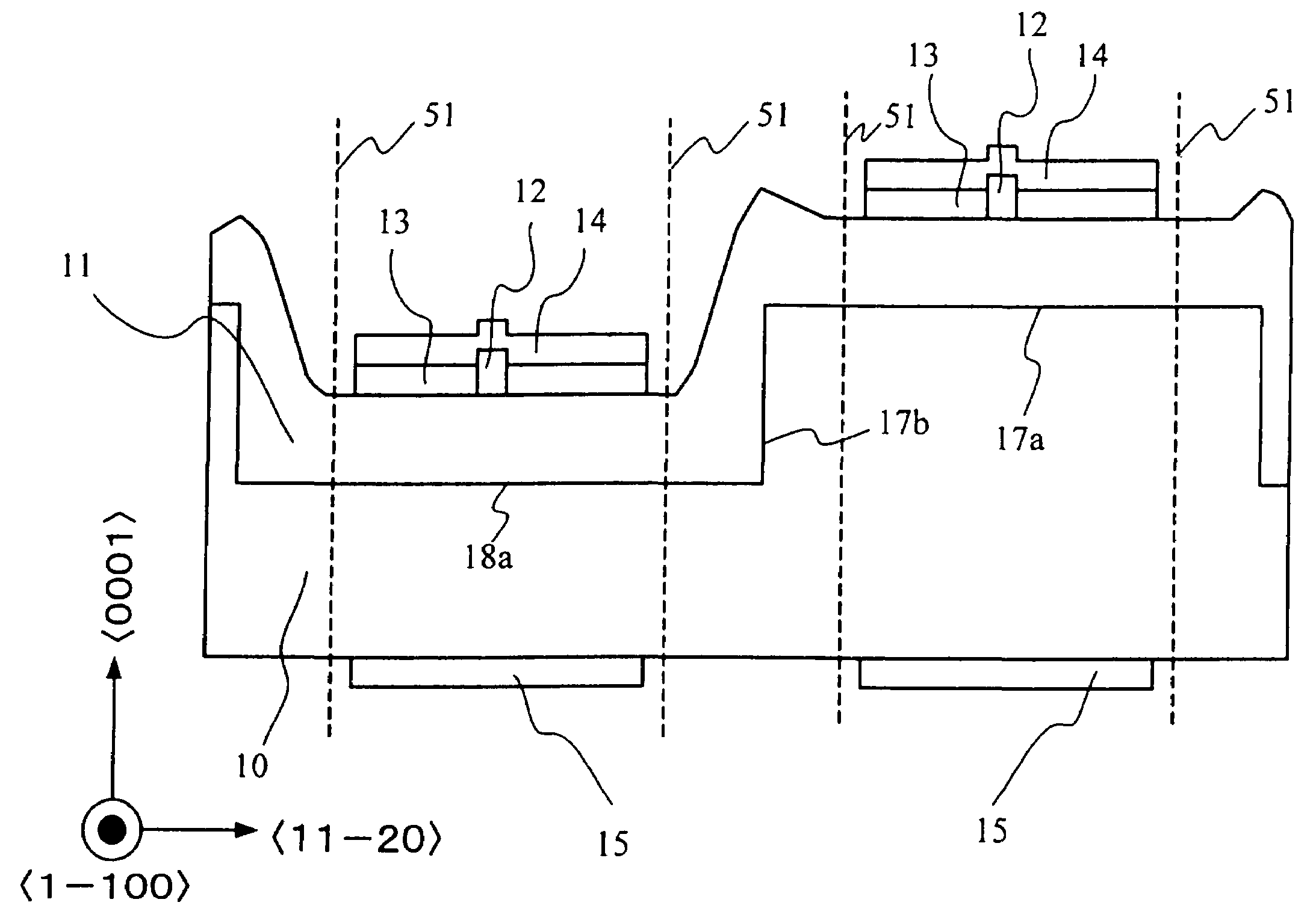
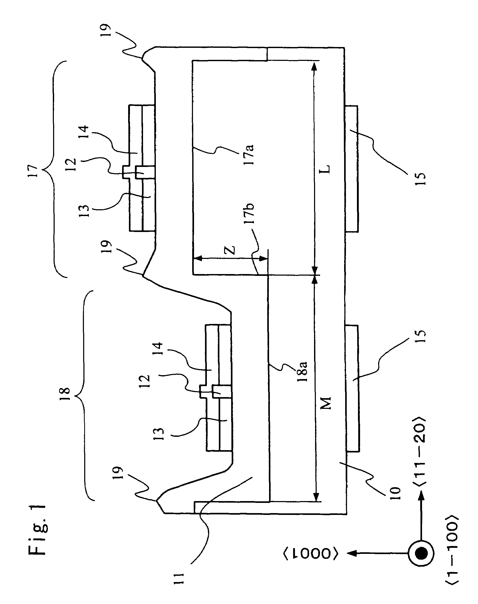
[0034]A first embodiment of the present invention will be described below with reference to the relevant drawings. The following description deals with, as an example of a nitride light-emitting device, a nitride semiconductor laser device. FIG. 1 is a schematic sectional view showing part of a wafer on which the nitride semiconductor laser device of this embodiment is formed. FIG. 2 is a top view of an n-type GaN substrate 10 as observed before a nitride semiconductor growth layer 11 is laid on top thereof in this embodiment. In these figures, plane orientations are indicated together. The nitride semiconductor laser device shown in FIG. 1 is produced by laying or otherwise forming a nitride semiconductor growth layer 11 on top of the n-type GaN substrate 10 shown in FIG. 2.

[0035]As shown in FIG. 2, on the n-type GaN substrate 10, ridges 17 and grooves 18 are formed in a direction parallel to the direction. Here, the ridges and grooves are assumed to have a rectangular cross-secti...

second embodiment

[0082]A second embodiment of the present invention will be described below with reference to the relevant drawings. FIG. 7 is a schematic sectional view showing part of a wafer on which the nitride semiconductor laser device of this embodiment is formed. In this embodiment, the nitride semiconductor growth layer 11 laid on top of the n-type GaN substrate 10 has the same structure as in FIG. 3 except for the layer thickness of the n-type GaN layer 21. Thus, here, the same reference numerals as used with the first embodiment are used, and, for detailed explanations that will be omitted in the description of this embodiment, the corresponding parts of the description of the first embodiment are to be referred to. Though not shown in FIG. 7, in this embodiment, the off angle of the n-type GaN substrate 10 relative to the principal plane orientation, i.e., the C plane (0001), is 0.2°.

[0083]The n-type GaN substrate 10 has grooves 18 and ridges 17 formed in a direction parallel to the dir...

third embodiment

[0093]A third embodiment of the present invention will be described below with reference to the relevant drawings. FIG. 8 is a schematic sectional view showing part of a wafer on which the nitride semiconductor laser device of this embodiment is formed. In this embodiment, the nitride semiconductor growth layer 11 laid on top of the n-type GaN substrate 10 has the same structure as in FIG. 3 except for the layer thickness of the n-type GaN layer 21. Thus, here, the same reference numerals as used with the first embodiment are used, and, for detailed explanations that will be omitted in the description of this embodiment, the corresponding parts of the description of the first embodiment are to be referred to. Though not shown in FIG. 8, in this embodiment, the off angle of the n-type GaN substrate 10 relative to the principal plane orientation, i.e., the C plane (0001), is just 0°.

[0094]In this embodiment, the n-type GaN substrate 10 has grooves 18 and ridges 17 formed in a directio...


PUM

PropertyMeasurementUnit
angleaaaaaaaaaa
thicknessaaaaaaaaaa
thicknessaaaaaaaaaa

Abstract

Provided is a method for fabricating a nitride semiconductor light-emitting device including a nitride semiconductor substrate having a groove and a ridge formed on the top surface thereof so as to extend in the shape of stripes and a nitride semiconductor growth layer consisting of a plurality of nitride semiconductor layers laid on top of the nitride semiconductor substrate. The method involves a step of forming a 10 μm or more wide flat region above at least either of the groove and ridge by forming the nitride semiconductor growth layer on top of the nitride semiconductor substrate so that the height of the nitride semiconductor growth layer laid above the groove is smaller than the height of the nitride semiconductor growth layer laid above the ridge.

Description

[0001]This nonprovisional application claims priority under 35 U.S.C. § 119(a) on Patent Application No. 2004-044630 filed in Japan on Feb. 20, 2004, the entire contents of which are hereby incorporated by reference.BACKGROUND OF THE INVENTION[0002]1. Field of the Invention[0003]The present invention relates to a nitride semiconductor light-emitting device such as a nitride semiconductor laser device.[0004]2. Description of Related Art[0005]Nitride semiconductor laser devices that lase in an ultraviolet to visible region of the spectrum have been fabricated on a commercial basis as well as on a trial basis by the use of nitride semiconductor materials exemplified by GaN, AlN, InN, and mixed crystals thereof. For this purpose, GaN substrates are typically used, the use of which, however, has thus far never led to the production of nitride semiconductor laser devices with satisfactorily long lasing lives. Thus, longer lasing lives are sought after. The lasing lives of nitride semicond...

Claims


Application Information

Patent Timeline
Patent Type & Authority Patents(United States)
IPC IPC(8): H01L21/00H01S5/02H01L21/20H01L21/205H01L21/306H01S5/20H01S5/22H01S5/223H01S5/30H01S5/323H01S5/343
CPCB82Y20/00H01L21/0243H01L21/02433H01L21/02458H01L21/02505H01L21/0254H01L33/007H01S5/2231H01S5/34333H01L21/02389H01S2304/04H01L21/30612H01S5/0202H01S5/2004H01S5/2201H01S5/2214H01S5/305
Inventor TAKAKURA, TERUYOSHIKAMIKAWA, TAKESHIKANEKO, YOSHIKA
Owner SHARP FUKUYAMA LASER CO LTD
Why Eureka
Try Eureka