Laser irradiating apparatus and method of manufacturing semiconductor apparatus

a technology of laser irradiation and semiconductor equipment, which is applied in the direction of manufacturing tools, chemical vapor deposition coatings, coatings, etc., can solve the problems of glass substrate deformation, significant difficulty in processing quartz substrates into a large area substrates, and lower melting points of glass substrates than those of quartz substrates

Inactive Publication Date: 2002-10-24
SEMICON ENERGY LAB CO LTD
View PDF54 Cites 71 Cited by
  • Summary
  • Abstract
  • Description
  • Claims
  • Application Information

AI Technical Summary

Problems solved by technology

However, it is significantly difficult for the quartz substrate to be processed into a big area substrate.
The use of the glass substrate has many advantages, but there is a problem that the melting point of the glass substrate is lower than that of the quartz substrate.
Since annealing the semiconductor film requires a higher temperature, there is a problem of deformation of the glass substrate when annealed.
Therefore, it is possible to heat an object in an unbalanced manner.
Therefore, by using the polycrystalline semiconductor film, an active-matrix type of liquid crystal display device (a semiconductor device in which thin film transistors (TFT) for driving pixels and for a

Method used


Image

  • Laser irradiating apparatus and method of manufacturing semiconductor apparatus
  • Laser irradiating apparatus and method of manufacturing semiconductor apparatus
  • Laser irradiating apparatus and method of manufacturing semiconductor apparatus

Examples


first experiment

[0105] First of all, a test sample was prepared in which a primary insulating film (silicon oxide nitride film 150 nm thick was formed, and an amorphous silicon film 54 nm thick is formed thereon by using plasma CVD method. Next, after coating solution containing 10 ppm nickel on a weight basis, thermal processing at 500.degree. C. was performed for one hour. Then, thermal processing at 550.degree. C. was performed for four hours for the crystallization. Thus, a silicon film having a crystalline structure was formed. Next, the surface of the semiconductor film was cleaned by noble hydrofluoric acid. Then, first laser light (excimer laser) was irradiated thereto in the air or in an atmosphere containing oxygen. Here, the energy density of the first laser light was 476 mj / cm.sup.2. Next, the oxidized film formed when the first laser light was irradiated was removed by noble hydrofluoric acid. Then, the second laser light with the variety of energy densities (476, 507, 537 and 567 mj / c...

first embodiment

[0138] An example of the present invention will be described with reference to FIGS. 16A to 16D. Here, an example is described where a method different from the crystallization method (crystallization method using nickel) described in the embodiment is used. More specifically, a method will be described in detail whereby a semiconductor film having an amorphous structure, which is provided on an insulating substrate, is annealed by laser.

[0139] First of all, a primary insulating film 1101 is formed on a glass substrate 1100 in accordance with the method in the embodiment. In this example, a two-layer structure is used for the primary insulating film 1101 provided on the glass substrate. However, a structure may be used where a single layer film, which is the insulating film itself, or at least two layers are stacked. As a first layer of the primary insulating film 1101, a first silicon oxide nitride film (compositional ratio:Si=32%, O=27%, N=24% and H=17%) is formed 50 nm thick by u...

second embodiment

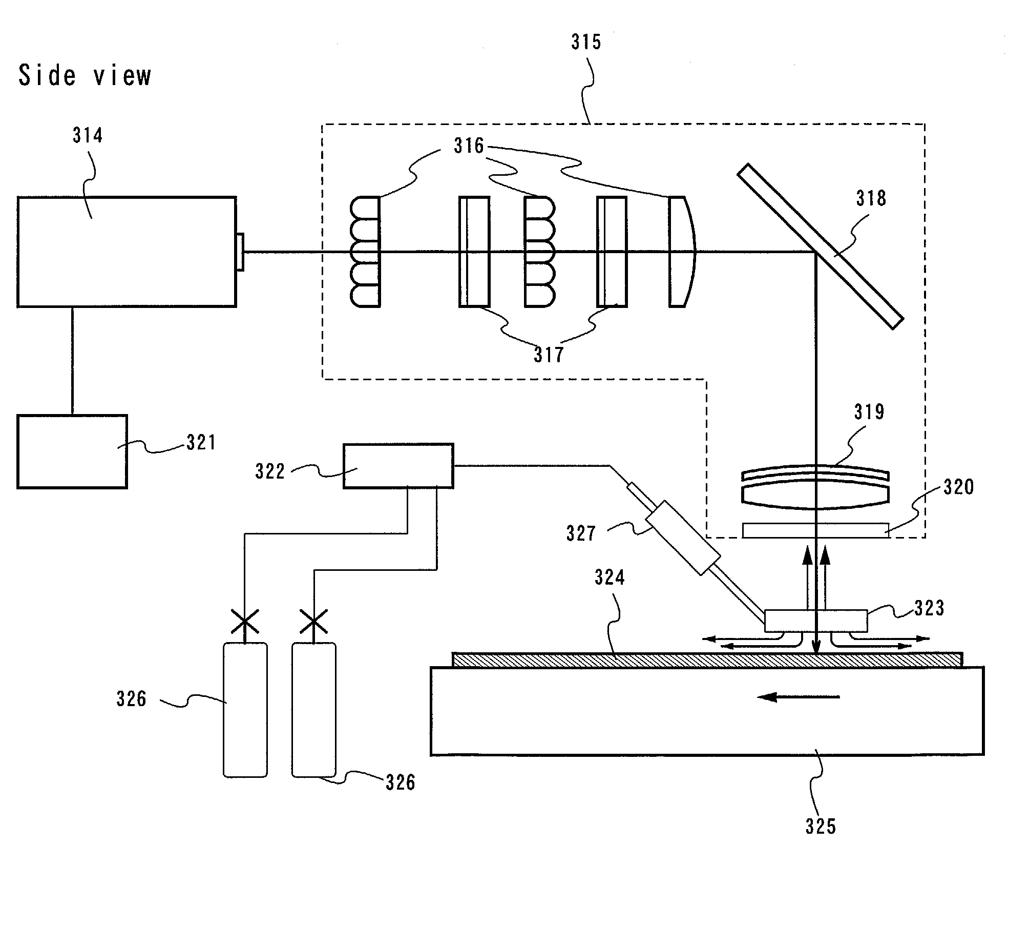
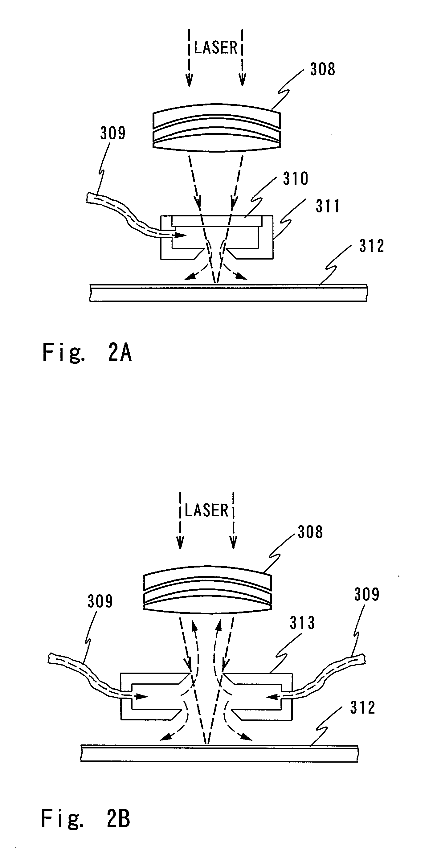
[0145] An example of a structure of a plate to which a gas is injected according to the present invention will be described with reference to FIGS. 2A and 2B.

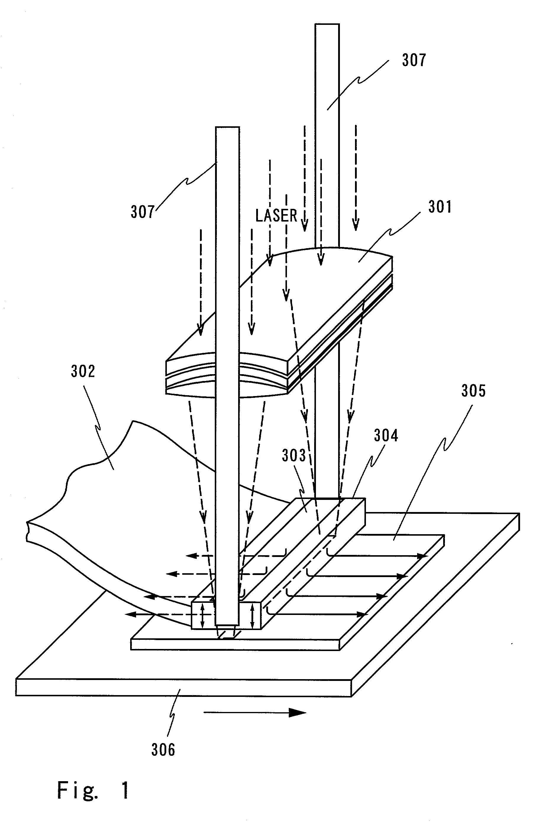
[0146] An example of a plate to which a gas is injected is shown in FIG. 2A. An inert gas is supplied from a gas feed tube 309 to a plate including a quartz window 310 and an aluminum alloy 311. The inert gas is injected from a slit-like hole provided at the bottom of the aluminum alloy 311. Under this condition, the plate in provided immediately above the semiconductor film 312 and is levitated by pressure caused by the injection of the inert gas.

[0147] A holding mechanism, not shown in FIG. 2A, for fixing a position of the plate, like the holding mechanism 307 shown in FIG. 1, must be provided. Thus, the plate can be levitated with stability above the semiconductor film 102. In the shown example, a triplet cylindrical lens 308 is used for gathering laser light linearly. By using this, laser light is gathered to the semiconduc...


PUM

PropertyMeasurementUnit
Fractionaaaaaaaaaa
Fractionaaaaaaaaaa
Angleaaaaaaaaaa

Abstract

First laser light is irradiated (energy density of 400 to 500 mj/cm2) to a semiconductor film 102 in an atmosphere containing oxygen in order to obtain a semiconductor film 102b having large depressions and projections on the surface. Then, an oxidized film 105a formed by the irradiation of the first laser light is removed. After that, an inert gas with an oxygen density of 10 ppm or below is blown thereto, and, at the same time, second laser light is irradiated thereto (the energy density is higher than that of the irradiation of the first laser light). Thus, the surface of the semiconductor film 102b is flattened, and a semiconductor film 102c having fewer depressions and projections on the surface can be obtained.

Description

[0001] 1. Field of the Invention[0002] The present invention relates to a method of manufacturing a semiconductor device, including a step of annealing a semiconductor film by using laser or equivalent strong light. The semiconductor apparatus refers to all of devices, which can function by using semiconductor characteristics and may be an electro-optical device, such as a liquid crystal display device, an electronic apparatus including an electro-optical device as its component, and a light emitting device.[0003] 2. Description of the Related Art[0004] A technology is widely known whereby laser annealing is performed on a semiconductor film formed on an insulating substrate, such as glass, for the crystallization, the improvement of crystalline characteristics, and / or the activation of dopant added to the semiconductor film. A silicon film may be used as the semiconductor film in many cases.[0005] A glass substrate may be used as the insulating substrate in many cases. The glass su...

Claims


Application Information

Patent Timeline
IPC IPC(8): B23K26/14H01L21/20H01L21/268H01L21/322H01L21/336
CPCB23K26/034B23K26/123B23K26/1435B23K26/1441Y10S438/935H01L21/2026H01L21/268H01L21/3226H01L29/66757B23K26/147B23K26/1436H01L21/02683H01L21/02502H01L21/02488H01L21/02422H01L21/02505H01L21/0242H01L21/02672H01L21/02425H01L21/02686H01L21/02678H01L21/02532H01L21/02381H01L21/02691
Inventor YAMAZAKI, SHUNPEITANAKA, KOICHIRO
Owner SEMICON ENERGY LAB CO LTD
Why Eureka
Try Eureka