Systems and methods for monolithically isled solar photovoltaic cells and modules

a solar photovoltaic and monolithic technology, applied in photovoltaic supports, power plants, sustainable buildings, etc., can solve the problems of thermally induced warpage crack generation and propagation, significant challenges and possible manufacturing yield degradation, and increase manufacturing cost and/or some manufacturing throughput and yield compromises, etc., to reduce or eliminate disadvantages and problems. , the effect of high efficiency

Inactive Publication Date: 2014-11-06
BEAMREACH SOLAR INC
View PDF17 Cites 73 Cited by
  • Summary
  • Abstract
  • Description
  • Claims
  • Application Information

AI Technical Summary

Benefits of technology

[0007]Therefore, a need has arisen for high efficiency solar cell fabrication methods and designs. In accordance with the disclosed subject matter, methods and structures for monolithically isled solar cells and modules are provided. These innovations substantially reduce or eliminate disadvantages and problems associated with previously developed solar cells.
[0009]Technical advantages of the innovative aspects disclosed herein include but are not limited to: enhanced flexibility and crack mitigation; reduced cell bow and improved planarity; scaled-up voltage and scaled-down cell current, resulting in reduced ohmic losses; and, a reduction in cell metallization thickness requirements.

Problems solved by technology

Current crystalline silicon (or other semiconductor absorber material) solar cell structures and processing methods often suffer from several disadvantages relating to cell bow and cell cracking / breakage during and / or after cell processing as well as during the operation of crystalline silicon PV modules installed in the field.
Solar cell processing often induces significant stresses (e.g., thermal and / or mechanical stresses) on a semiconductor substrate which may lead to thermally-induced warpage and crack generation and propagation (by thermal cycling or mechanical stresses).
Bowed or non-planar solar cell substrates pose significant challenges and possible manufacturing yield degradation during solar cell processing (such as during processing of crystalline silicon solar cells), and may present requirements for clamping down the solar cell substrate and / or the substrate edges onto a supporting substrate carrier to flatten the cell substrate during manufacturing process.
Flattening solutions may complicate the solar cell manufacturing process, resulting in increased manufacturing cost and / or some manufacturing throughput and yield compromises.
Bowed or non-planar solar cell substrates may further result in cell microcracks and / or breakage problems during module lamination and also subsequently during the PV module operation in the field (resulting in PV module power degradation or loss).
Further, conventional solar cells, particularly those based on an interdigitated back-contact or IBC design, often require relatively thick metallization patterns—due to the relatively high cell electrical current—which may add complexity to cell processing, increase material costs, and add significant physical stresses to the cell semiconductor material.
Such shade-induced hot-spot phenomena, which are caused by reverse biasing of the shaded cell or cells in a PV module, may permanently damage the affected PV cells as well as the PV module encapsulation material and cell-to-cell interconnections, and even cause fire hazards, if the sunlight arriving at the surface of the PV cells in a PV module is partially blocked or not sufficiently uniform within the PV module—for instance, due to full or even partial shading of one or a plurality of solar cells.
While the external bypass diodes (typically three external bypass diodes included in the standard mainstream 60-cell crystalline silicon PV module junction box) protect the PV module and cells in case of shading of the cells, they can also actually result in significant loss of power harvesting and energy yield for the installed PV systems.

Method used


Image

  • Systems and methods for monolithically isled solar photovoltaic cells and modules
  • Systems and methods for monolithically isled solar photovoltaic cells and modules
  • Systems and methods for monolithically isled solar photovoltaic cells and modules

Examples


Embodiment Construction

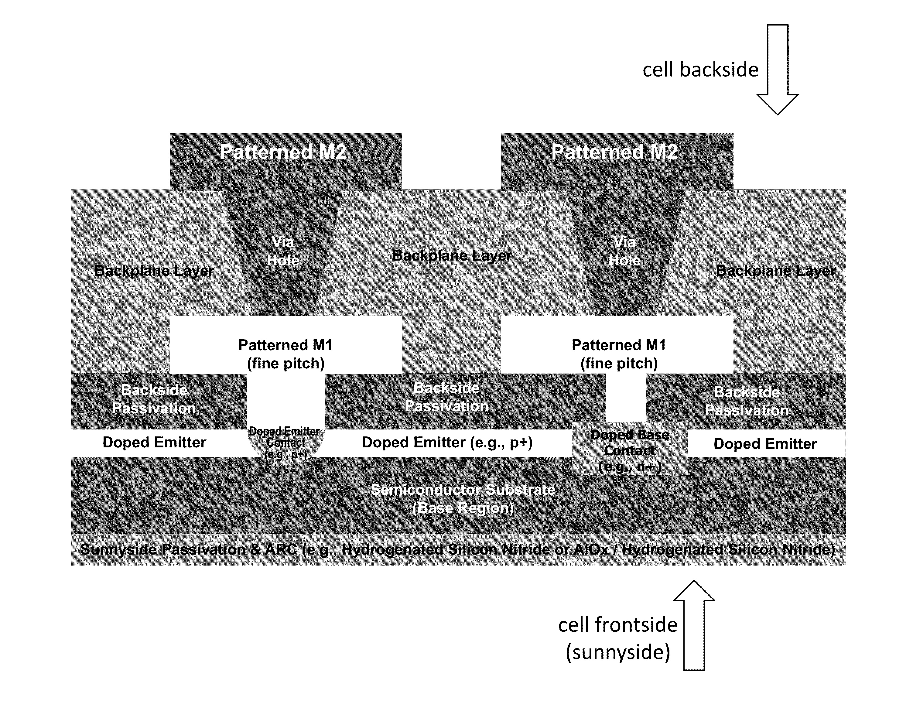
[0042]The following description is not to be taken in a limiting sense, but is made for the purpose of describing the general principles of the present disclosure. The scope of the present disclosure should be determined with reference to the claims. Exemplary embodiments of the present disclosure are illustrated in the drawings, like numbers being used to refer to like and corresponding parts of the various drawings.

[0043]Importantly, the exemplary dimensions and calculations disclosed for embodiments are provided both as detailed descriptions for specific embodiments and to be used as general guidelines when forming and designing solar cells in accordance with the disclosed subject matter.

[0044]And although the present disclosure is described with reference to specific embodiments, such as backplane-attached / back-contact solar cells such as interdigitated back-contact (IBC) solar cells using monocrystalline silicon substrates and other described fabrication materials, one skilled ...


PUM


Abstract

According to one aspect of the disclosed subject matter, a monolithically isled solar cell is provided. The solar cell comprises a semiconductor layer having a light receiving frontside and a backside opposite the frontside and attached to an electrically insulating backplane. A trench isolation pattern partitions the semiconductor layer into electrically isolated isles on the electrically insulating backplane. A first metal layer having base and emitter electrodes is positioned on the semiconductor layer backside. A patterned second metal layer providing cell interconnection and connected to the first metal layer by via plugs is positioned on the backplane.

Description

CROSS-REFERENCE TO RELATED APPLICATIONS[0001]This application claims the benefit of provisional patent application 61 / 722,620 filed on Nov. 5, 2012, which is hereby incorporated by reference in its entirety.FIELD OF THE INVENTION[0002]The present disclosure relates in general to the fields of solar photovoltaic (PV) cells and modules, and more particularly to monolithically isled or tiled photovoltaic (PV) solar cells and associated modules providing numerous benefits.BACKGROUND[0003]Crystalline silicon photovoltaic (PV) modules, as of 2012, account for approximately at least 85% of the overall global PV annual demand market and cumulative globally installed PV capacity. The manufacturing process for crystalline silicon PV is based on the use of crystalline silicon solar cells, starting with mono-crystalline or multi-crystalline silicon wafers made of czochralski (CZ) silicon ingots or cast silicon bricks. Non-crystalline-silicon-based thin film PV modules (for example CdTe, CIGS, o...

Claims


Application Information

Patent Timeline
Patent Type & Authority Applications(United States)
IPC IPC(8): H01L31/0224H01L27/142H01L31/18
CPCH01L31/02245H01L27/1421H01L31/18H01L31/0516H01L31/02H01L31/0201H01L31/022433H01L31/0504H01L31/1896H01L31/0445H01L31/0443Y02E10/547Y02B10/10Y02E10/56Y02E10/50H02S20/25H02S40/34H01L31/048
Inventor MOSLEHI, MEHRDAD M.
Owner BEAMREACH SOLAR INC
Why Eureka
Try Eureka