Ligth-emitting element, light-emitting device, and electronic device

a technology of light-emitting elements and ligth-emitting elements, which is applied in the direction of discharge tube/lamp details, organic semiconductor devices, discharge tubes luminescnet screens, etc., can solve the problems of short life of light-emitting elements and cannot be easily achieved, so as to reduce power consumption, suppress changes in carrier balance over time, and high luminous efficiency

Active Publication Date: 2008-01-10
SEMICON ENERGY LAB CO LTD
View PDF8 Cites 54 Cited by
  • Summary
  • Abstract
  • Description
  • Claims
  • Application Information

AI Technical Summary

Benefits of technology

[0021] The light-emitting element of the invention has a layer for controlling the movement of carriers, whereby changes in carrier balance over time can be suppressed. Therefore, a long-lifetime light-emitting element can be obtained. Further, when the light-emitting element of the invention is applied to a light-emitting device and an electronic device, it is possible to provide a light-emitting device and an electronic device having high luminous efficiency and reduced power consumption. In addition, a light-emitting device and electronic device having a long lifetime can be obtained.

Problems solved by technology

This cannot be easily achieved with a point light source typified by an incandescent lamp or an LED, or with a line light source typified by a fluorescent lamp.
However, since the hole blocking layer disclosed in Reference 1 is not durable, the light-emitting element has a short lifetime.

Method used


Image

  • Ligth-emitting element, light-emitting device, and electronic device
  • Ligth-emitting element, light-emitting device, and electronic device
  • Ligth-emitting element, light-emitting device, and electronic device

Examples


embodiment mode 1

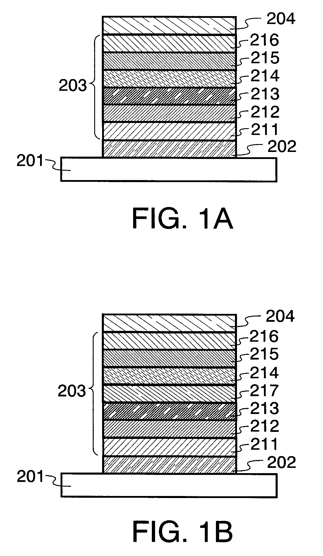
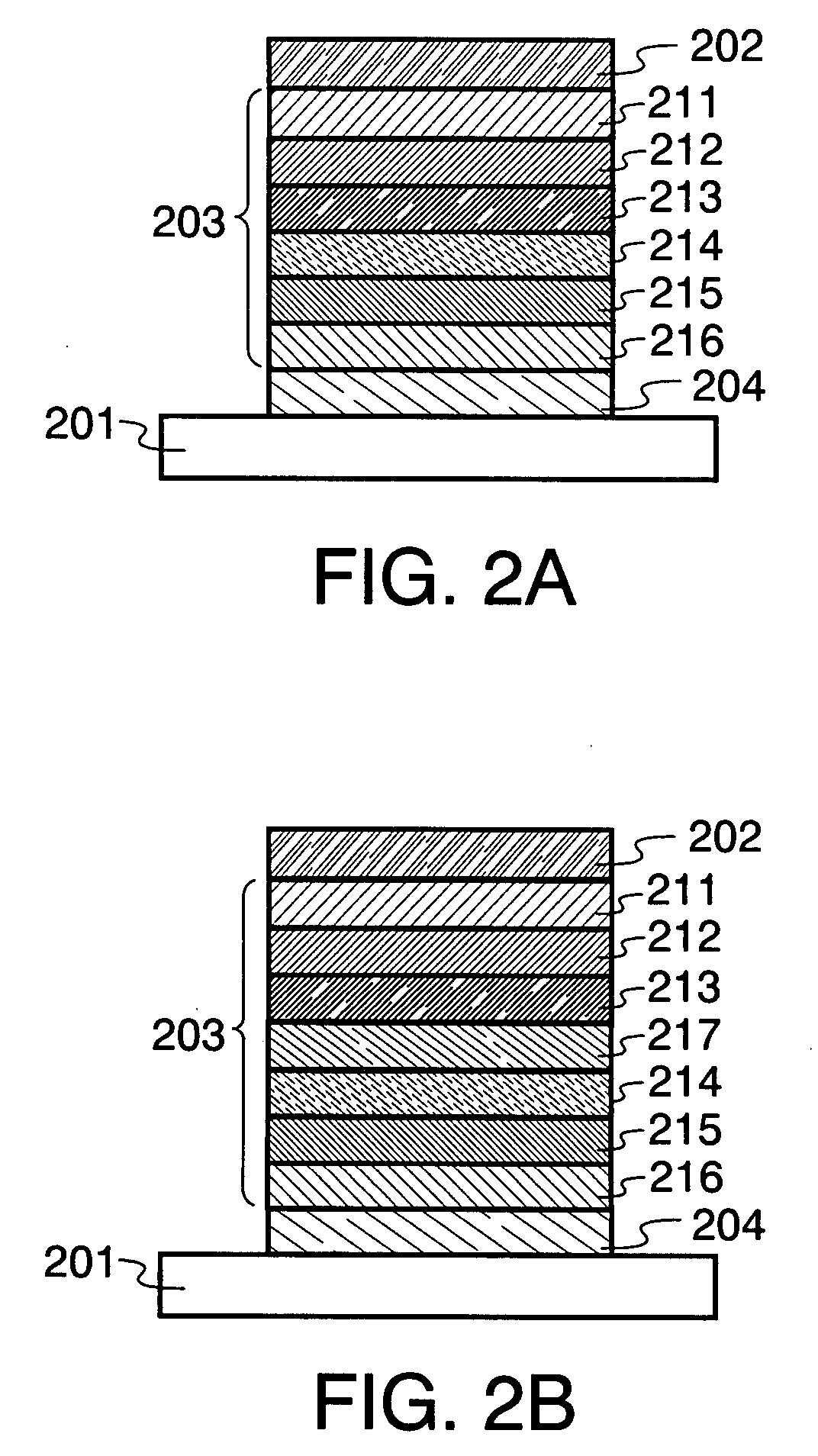
[0091] One example of a light-emitting element of the invention will be described with reference to FIG. 1A. This embodiment mode illustrates a light-emitting element which includes a layer for controlling the movement of electrons as a layer for controlling the movement of carriers. That is, in the invention, changes in carrier balance over time are suppressed by using the layer for controlling the movement of carriers, so that the carriers are recombined at a position away from electrodes, whereby the lifetime of the light-emitting element is prolonged.

[0092] The light-emitting element of the invention has a plurality of layers between a pair of electrodes. The plurality of layers is stacked by combining layers made of a compound with a high carrier injection property and a compound with a high carrier transporting property so that a light-emitting region is formed at a position away from the electrodes, i.e., so that carriers are recombined at a position away from the electrodes...

embodiment mode 2

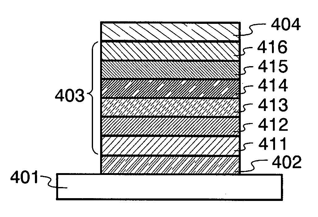
[0176] This embodiment mode will describe one example of a light-emitting element of the invention which differs from that shown in Embodiment Mode 1, with reference to FIG. 5A. This embodiment mode illustrates a light-emitting element which includes a layer for controlling the movement of holes as a layer for controlling the movement of carriers. The light-emitting element of the invention has a plurality of layers between a pair of electrodes. The plurality of layers is stacked by combining layers made of a compound with a high carrier injection property and a compound with a high carrier transporting property so that a light-emitting region is formed at a position away from the electrodes, i.e., so that carriers are recombined at a position away from the electrodes.

[0177] In this embodiment mode, a light-emitting element includes a first electrode 402, a second electrode 404, and an EL layer 403 provided between the first electrode 402 and the second electrode 404. Note that in ...

embodiment mode 3

[0225] This embodiment mode will describe a light-emitting element in which a plurality of light-emitting units in accordance with the invention is stacked, with reference to FIG. 9. The light-emitting element is a stacked-type light-emitting element which has a plurality of light-emitting units between a first electrode and a second electrode. A structure similar to that of the EL layer 203 shown in Embodiment Mode 1 or the EL layer 403 shown in Embodiment Mode 2 can be used for each light-emitting unit. In other words, the light-emitting element described in each of Embodiment Modes 1 and 2 is a light-emitting element having a single light-emitting unit. In this embodiment mode, a light-emitting element having a plurality of light-emitting units will be described.

[0226] In FIG. 9, a first light-emitting unit 511 and a second light-emitting unit 512 are stacked between a first electrode 501 and a second electrode 502. A charge generation layer 513 is provided between the first lig...


PUM


Abstract

The light-emitting element includes: a light-emitting layer and a layer for controlling the movement of carriers between a first electrode and a second electrode. The layer for controlling the movement of carriers contains a first organic compound and a second organic compound, and is provided between the light-emitting layer and the second electrode. The first organic compound has an electron transporting property, and the second organic compound has an electron trapping property. The weight percent of the first organic compound is higher than that of the second organic compound. The light-emitting layer emits light when a voltage is applied such that the potential of the first electrode is higher than that of the second electrode. The first organic compound having the electron transporting property may be replaced with an organic compound having a hole transporting property, and the second organic compound having the electron trapping property may be replaced with an organic compound having a hole trapping property.

Description

BACKGROUND OF THE INVENTION [0001] 1. Field of the Invention [0002] The present invention relates to current-excitation light-emitting elements, and also relates to light-emitting devices and electronic devices having such light-emitting elements. [0003] 2. Description of the Related Art [0004] In recent years, a light-emitting element utilizing electroluminescence has actively been researched and developed. The basic structure of the light-emitting element is such that a light-emissive compound is sandwiched between a pair of electrodes. By applying a voltage to such an element, light emission can be obtained from the light-emissive compound. [0005] Such a light-emitting element which is a self-luminous type has an advantage in that it has higher visibility of pixels than liquid crystal displays, and there is no need to use a backlight. Thus, such a light-emitting element is considered to be suitable for a flat panel display element. Besides, such a light-emitting element has advan...

Claims


Application Information

Patent Timeline
Patent Type & Authority Applications(United States)
IPC IPC(8): H01L51/50H05B33/12
CPCH01L51/5096H01L2251/552H01L51/5076H01L51/506H01L2251/558H10K50/155H10K50/165H10K50/18H10K2101/30H10K2102/351H10K50/11H10K50/16H10K50/805H10K50/14H10K50/157H10K50/167
Inventor SUZUKI, TSUNENORISEO, SATOSHINOMURA, RYOJI
Owner SEMICON ENERGY LAB CO LTD
Why Eureka
Try Eureka