Vertical gallium nitride based nitride heterojunction field effect transistor with polarized doped current barrier layer

A heterojunction field effect, current blocking layer technology, applied in circuits, electrical components, semiconductor devices, etc., can solve the problems of reduced p-type impurity activation rate, low activation energy, low p-type impurity activation rate, etc. Thermal stability and reliability, leakage current suppression, high band gap effect

Inactive Publication Date: 2013-04-10
UNIV OF ELECTRONICS SCI & TECH OF CHINA
View PDF1 Cites 28 Cited by
  • Summary
  • Abstract
  • Description
  • Claims
  • Application Information

AI Technical Summary

Problems solved by technology

Among the known p-type impurities in GaN materials, the Mg impurity has the lowest activation energy, about 200meV, but it is still much higher than the thermoelectric potential (about 26meV) at room temperature. Excessively high impurity activation energy leads to The activation rate of p-type impurities is very low, only about 1%, and it will decrease sharply with the decrease of temperature. When the material is AlGaN or AlN, the activation rate of p-type impurities will further decrease due to the further increase of activation energy.

Method used


Image

  • Vertical gallium nitride based nitride heterojunction field effect transistor with polarized doped current barrier layer
  • Vertical gallium nitride based nitride heterojunction field effect transistor with polarized doped current barrier layer
  • Vertical gallium nitride based nitride heterojunction field effect transistor with polarized doped current barrier layer

Examples


Embodiment

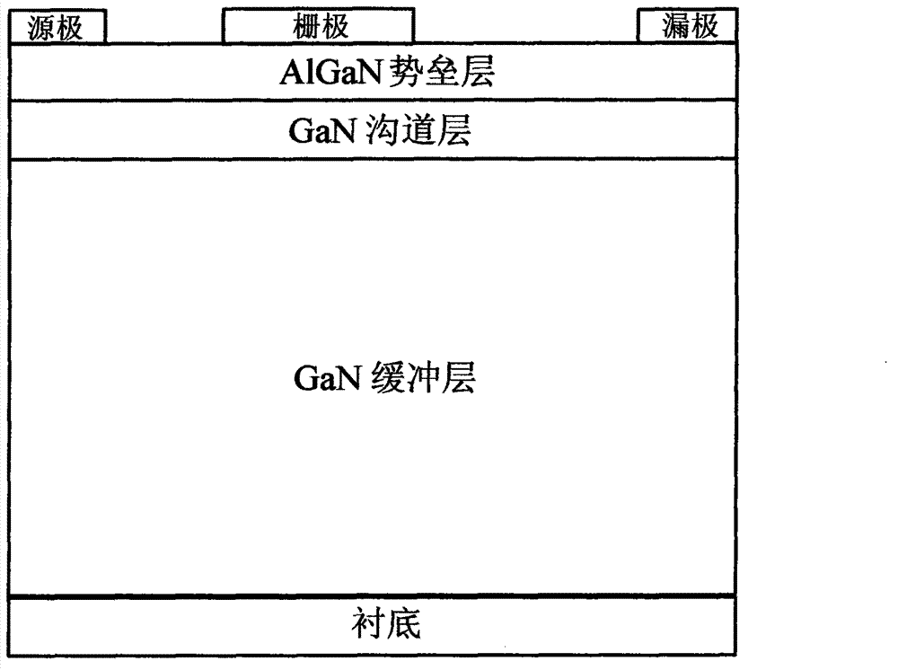
[0027] figure 1 It is a schematic diagram of the horizontal GaN HFET structure in the prior art, which mainly includes a substrate, a gallium nitride (GaN) buffer layer, a gallium nitride (GaN) channel layer, an aluminum gallium nitride (AlGaN) barrier layer and an aluminum gallium nitride (AlGaN) barrier layer from bottom to top The source, drain and gate formed on the (AlGaN) barrier layer, wherein the source and drain form ohmic contacts with the aluminum gallium nitride (AlGaN) barrier layer, and the gate contacts with the aluminum gallium nitride (AlGaN) barrier layer form a Schottky contact.

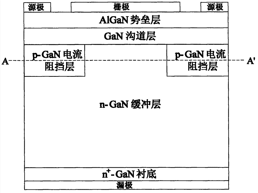
[0028] figure 2It is a schematic diagram of the GaN VHFET structure in the prior art, mainly including the drain from bottom to top, n + -GaN substrate, n-GaN buffer layer, p-GaN current blocking layer, GaN channel layer, AlGaN barrier layer, and source and gate formed on the AlGaN barrier layer, wherein the source and drain are ohmic contact, the gate is a Schottky contact.

...


PUM


Abstract

The invention provides a vertical gallium nitride based nitride heterojunction field effect transistor with a polarized doped current barrier layer, which sequentially and mainly comprises a drain electrode, an n<+>-GaN substrate, an n-GaN buffer layer, a GaN channel layer, an AlGaN barrier layer, a source electrode on the AlGaN barrier layer and a grid electrode on the AlGaN barrier layer from bottom to top, wherein the source electrode and the drain electrode are both in ohmic contact, the grid electrode is in Schottky contact, the vertical gallium nitride based nitride heterojunction field effect transistor further comprises the polarized doped p-AlGaN current barrier layer between the n-GaN buffer layer and the GaN channel layer, and an Al component in the current barrier layer increases gradually in the y direction. According to the vertical gallium nitride based nitride heterojunction field effect transistor with the polarized doped current barrier layer, a polarized electric field, produced by the gradual change of the Al component in the current barrier layer, increases the activation rate of p-type impurities and the hole concentration of the current barrier layer, so that the breakdown voltage of an element is increased.

Description

technical field [0001] The invention relates to the field of semiconductor devices, in particular to a vertical GaN-based heterojunction field effect transistor with a polarized doped current blocking layer. technical background [0002] Gallium nitride-based heterojunction field effect transistor (Heterojunction Fiele-Effect Transistor, HFET) not only has a large band gap, a high critical breakdown electric field, a high electron saturation velocity, good thermal conductivity, radiation resistance and good chemical stability, etc. Excellent characteristics, at the same time gallium nitride (GaN) materials can form a two-dimensional electron gas heterojunction channel with high concentration and high mobility with materials such as aluminum gallium nitride (AlGaN), so it is especially suitable for high voltage, high power and high temperature It is one of the most potential transistors for power electronics applications. [0003] The existing high withstand voltage GaN HFET...

Claims


Application Information

Patent Timeline
Patent Type & Authority Applications(China)
IPC IPC(8): H01L29/778H01L29/06
Inventor 杜江锋赵子奇罗杰尹成功严慧黄思霓罗谦于奇
Owner UNIV OF ELECTRONICS SCI & TECH OF CHINA
Why Eureka
Try Eureka