

Magnetoresistive element, magnetic head, magnetic memory and magnetic recording apparatus using the same
- Summary
- Abstract
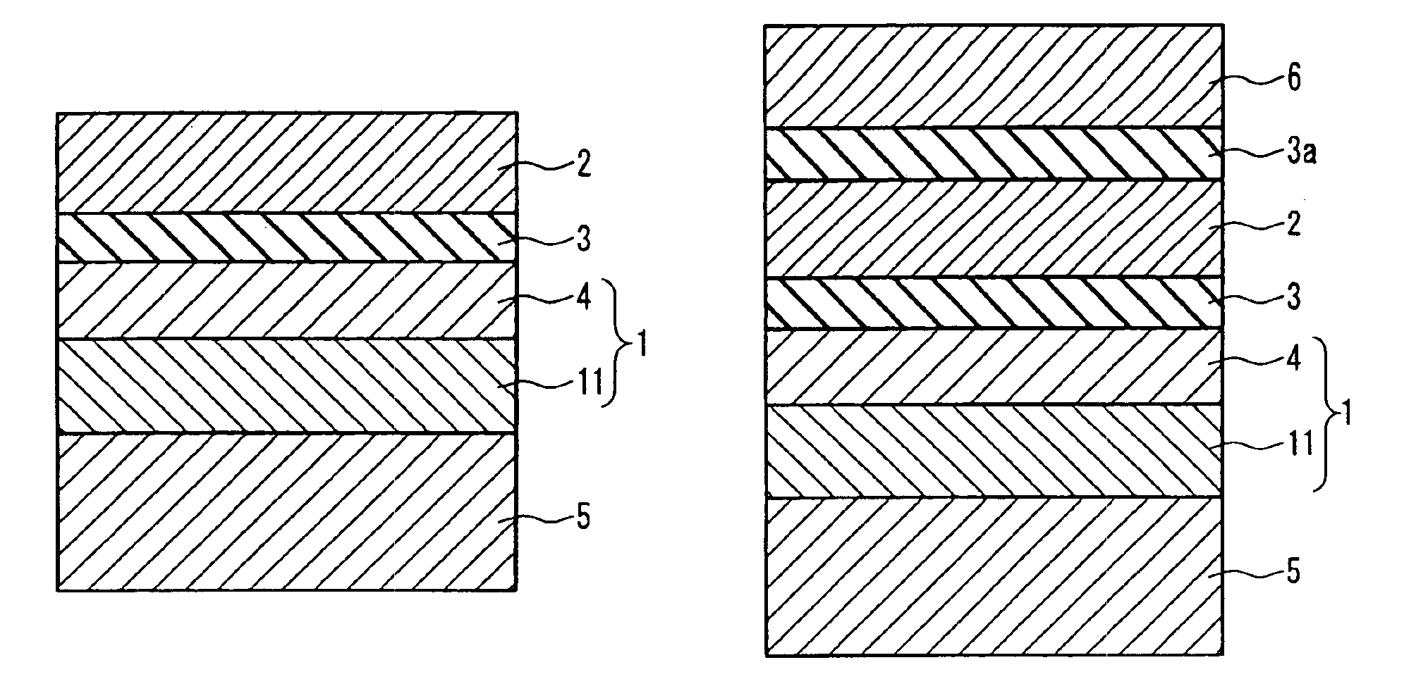
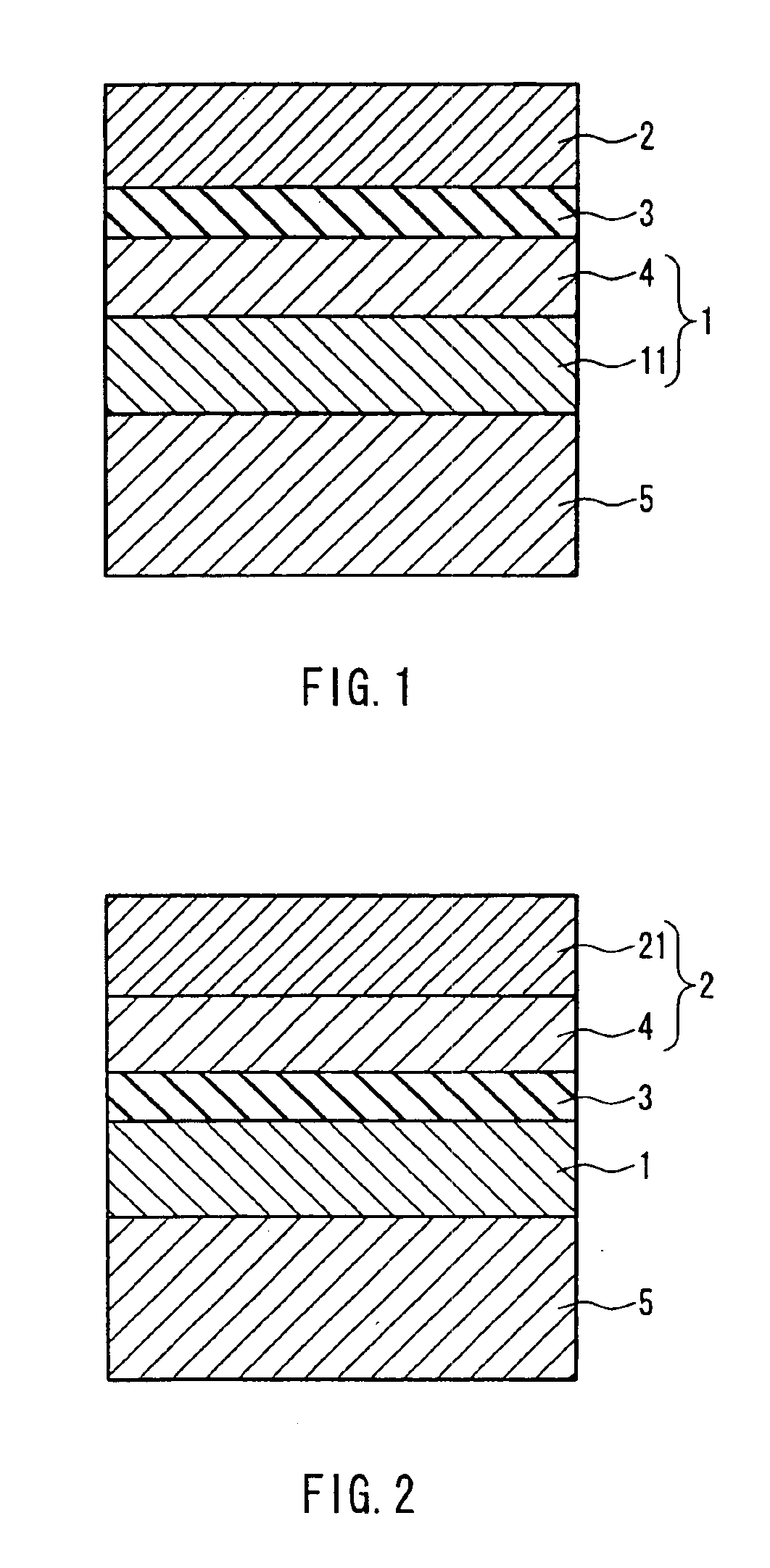
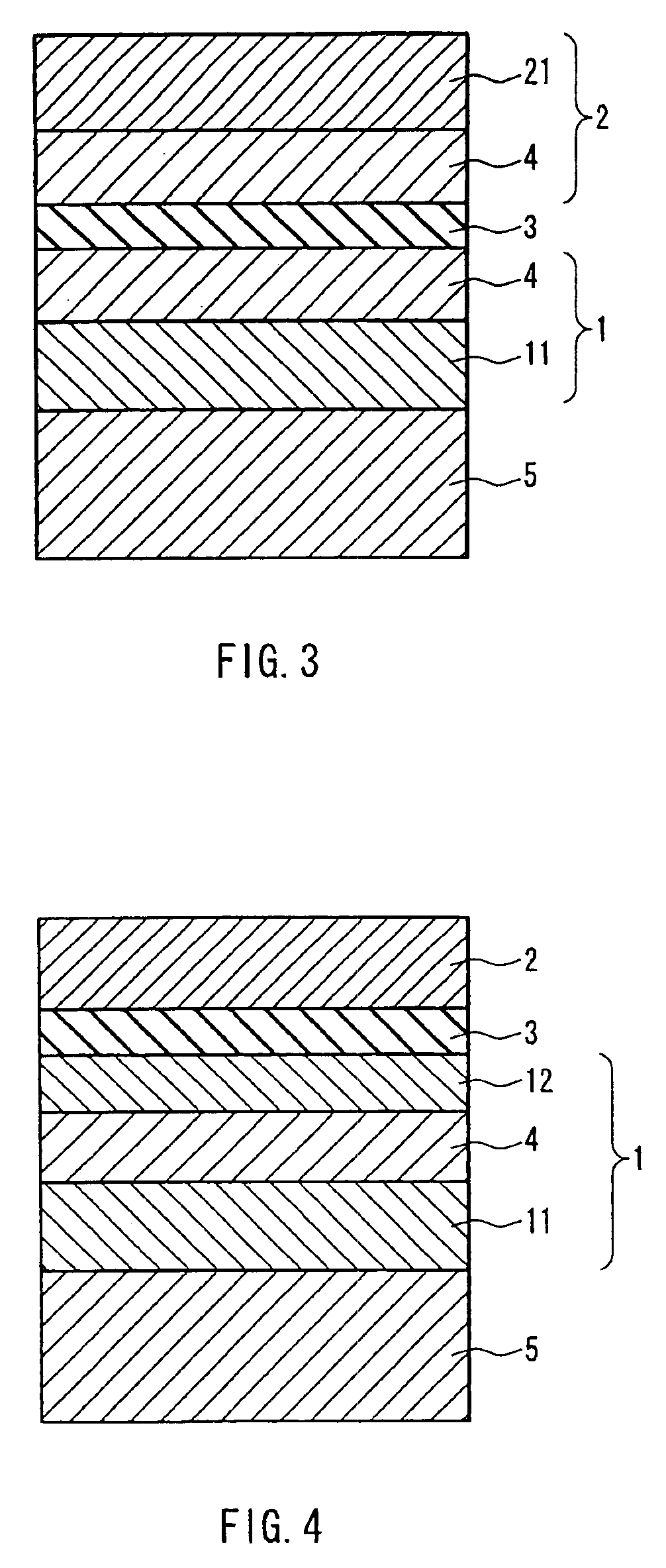
- Description
- Claims
- Application Information
AI Technical Summary
Benefits of technology
Problems solved by technology
Method used
Image

Examples
example 1
Si substrate with a thermal oxide film / Ta (3) / Cu (50) / Ta (3) / Pt—Mn (30) / Co—Fe (1) / X / Al2O3 (0.6) / Ni0.8Fe0.2 (5)
The figure in parentheses represents the thickness of each layer in nm, and the film thickness is expressed in the same manner in the following. However, the figure for Al2O3 is a designed thickness (total value) for Al prior to the oxidation procedure (the same applies to the following, including a nitride procedure for AlN). Al2O3 was produced by forming an Al film with a thickness of 0.3 to 0.7 nm, followed by repeated oxidation for 1 minute in an atmosphere containing oxygen at 26.3 kPa (200 Torr).
Ta (3) / Cu (50) on the substrate serves as a lower electrode, and Ta (3) between the lower electrode and the Pt—Mn layer serves as a buffer layer. The Pt—Mn layer is an antiferromagnetic layer, and the MR element of this example is a spin valve type MR element. Note here that the compositions of the Pt—Mn layer and the Co—Fe layer are Pt0.48Mn0.52 and Co0.75Fe0.25, respectively....
example 2
In this example, as for a MR element in which a low thermal expansion magnetic film made of an invar alloy was arranged on either surface of a tunnel insulation layer, the dependency of the MR properties on the heat treatment temperature was evaluated.
By the method similar to Example 1, MR elements with the following film configuration were produced.
Si substrate with a thermal oxide film / Ta (3) / Cu (50) / Ta (3) / Ni—Fe—Cr (4) / Pt—Mn (20) / Co—Fe (3) / Ru (0.8) / Co—Fe (1) / X1 / Al2O3 (1) / X2 / Ni0.8Fe0.2 (5)
Ta (3) / Cu (50) on the substrate serves as a lower electrode, and Ta (3) / Ni—Fe—Cr (4) between the lower electrode and the Pt—Mn (20) serves as a buffer layer. The Pt—Mn layer is an antiferromagnetic layer, and the Co—Fe (3) / Ru (0.8) / Co—Fe (1) is a synthetic ferrimagnetic structure, where Ru is a non-magnetic film.
X1 and X2 denote magnetic materials having the compositions shown in the following Table 2. In this example, one type of sample was prepared as a conventional example (sample b01), wherea...
example 3
In this example, as for a MR element in which AlN was used for a tunnel insulation layer, the dependency of the MR properties on the heat treatment temperature was evaluated.
By the method similar to Example 1, MR elements with the following film configuration were produced.
Si substrate with a thermal oxide film / Ta (3) / Cu (50) / Ta (3) / Ni—Fe (4) / X / AlN (1.3) / X / Co (5) / Ir—Mn (8)
Ta (3) / Cu (50) on the substrate serves as a lower electrode, and Ta (3) between the lower electrode and the Ni—Fe layer serves as a buffer layer. The Ir—Mn layer is an antiferromagnetic layer. X denotes magnetic materials having the compositions shown in the following Table 4. In this example, one type of sample was prepared as a conventional example (sample c01), whereas four types of samples were prepared for this example (samples c02 to c05), which had the element size of 2 μm×4 μm. Note here that the compositions of the Ni—Fe layer and the Ir—Mn layer were Ni0.8Fe0.2 and Ir0.2Mn0.8, respectively.
AlN functioning...
PUM
 Abstract
Description
Claims
Application Information