Nitride semiconductor device and manufacturing method thereof

a technology of semiconductor devices and semiconductors, applied in semiconductor devices, basic electric elements, electrical equipment, etc., can solve the problems of increased leakage current of gate terminals and limited gate voltage sweep range, and achieve the effect of suppressing gate leakage curren

Active Publication Date: 2013-04-04
SAMSUNG ELECTRO MECHANICS CO LTD
View PDF2 Cites 27 Cited by
  • Summary
  • Abstract
  • Description
  • Claims
  • Application Information

AI Technical Summary

Benefits of technology

[0011]The present invention has been invented in order to overcome the above-described problems and it is, therefore, an object of the present invention to provide a nit...

Problems solved by technology

However, in a conventional gate structure using p-type GaN, there is a disadvantage that leakage current of a gate terminal is increased during turn-on operation or a gate vol...

Method used


Image

  • Nitride semiconductor device and manufacturing method thereof
  • Nitride semiconductor device and manufacturing method thereof
  • Nitride semiconductor device and manufacturing method thereof

Examples


first embodiment

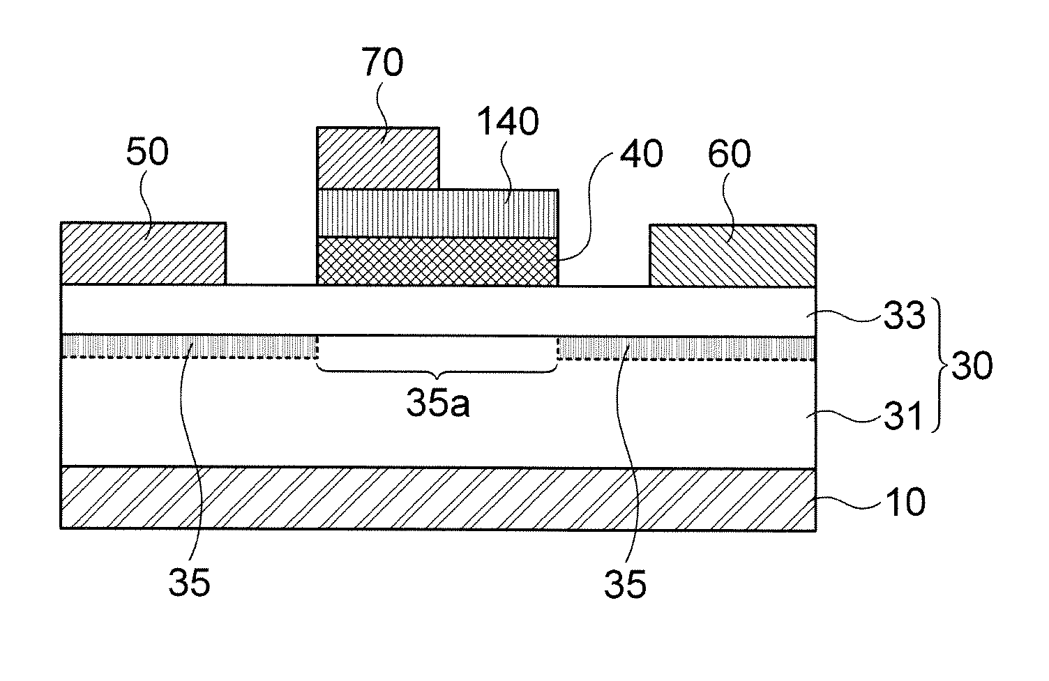
[0036]First, a nitride semiconductor device in accordance with the present invention will be described with reference to FIGS. 1 and 3.

[0037]Referring to FIGS. 1 and 3, a nitride semiconductor device in accordance with an example includes a nitride semiconductor layer 30, a source electrode 50, a drain electrode 60, a p-type nitride layer 40, an n-type nitride layer 140, and a gate electrode 70. At this time, in an example, the nitride semiconductor device may be a power transistor device.

[0038]Referring to FIGS. 1 and 3, the nitride semiconductor layer 30 is formed by a heterojunction of a first nitride layer 31 and a second nitride layer 33 which includes a material with a wider energy band gap than a material of the first nitride layer 31. A two-dimensional electron gas (2DEG) channel 35 is formed near a junction interface of the nitride semiconductor layer 30. The nitride semiconductor layer 30 is a heterojunction gallium nitride semiconductor layer, and the 2DEG channel 35 is f...

second embodiment

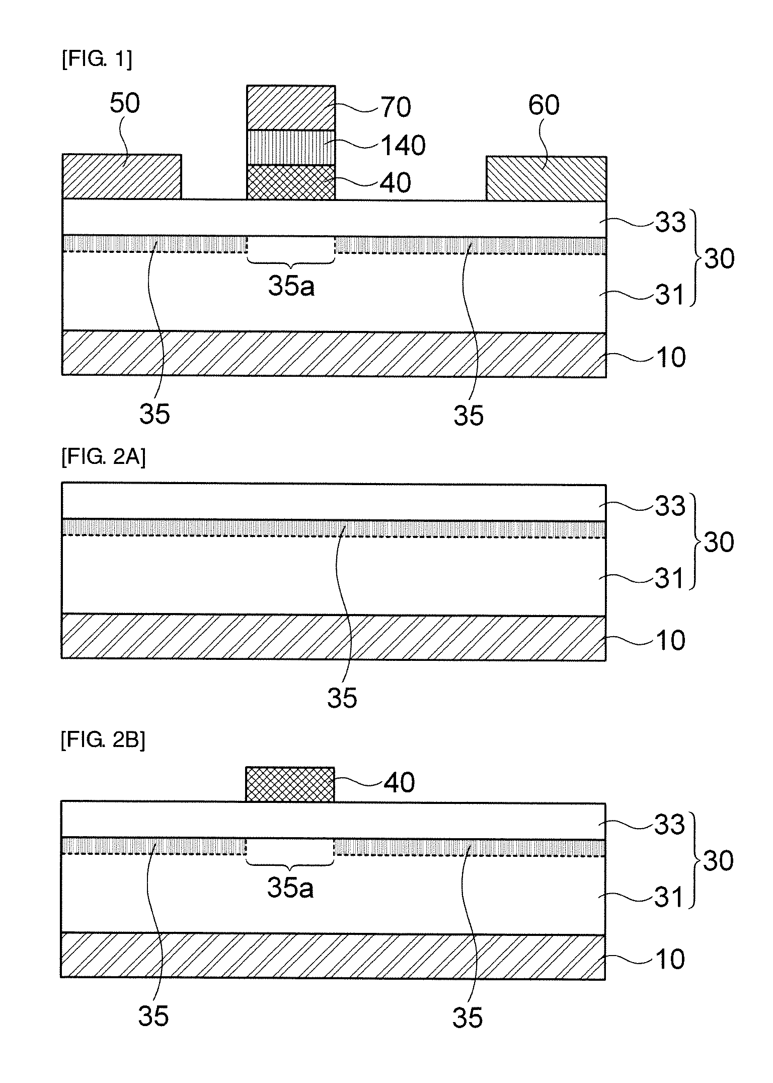
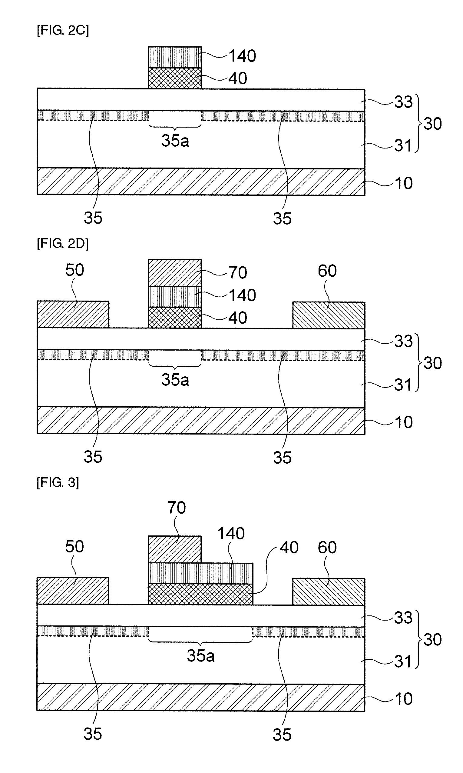
[0060]Next, a method of manufacturing a nitride semiconductor device in accordance with a second embodiment will be described with reference to FIGS. 2a to 2d. At this time, the embodiments of the above-described nitride semiconductor device and FIGS. 1 and 3 will be referenced. Accordingly, repeated description will be omitted.

[0061]Referring to FIGS. 2a to 2d, a method of manufacturing a nitride semiconductor device includes a heterojunction nitride semiconductor layer forming step, a p-type nitride layer forming step, an n-type nitride layer forming step, and an electrode forming step. At this time, in an example, the nitride semiconductor device may be a power transistor device.

[0062]Referring to FIG. 2a, in the heterojunction nitride semiconductor layer forming step, a nitride semiconductor layer 30 is formed by a heterojunction of a first nitride layer 31 and a second nitride layer 33 which includes a material with a wider energy band gap than a material of the first nitride l...


PUM


Abstract

The present invention relates to a nitride semiconductor device and a manufacturing method thereof. According to one aspect of the present invention, a nitride semiconductor device including: a nitride semiconductor layer having a 2DEG channel; a source electrode in ohmic contact with the nitride semiconductor layer; a drain electrode in ohmic contact with the nitride semiconductor layer; a p-type nitride layer formed on the nitride semiconductor layer between the source and drain electrodes; an n-type nitride layer formed on the p-type nitride layer; and a gate electrode formed between the source and drain electrodes to be close to the source electrode and in contact with the n-type nitride layer so that a source-side sidewall thereof is aligned with source-side sidewalls of the p-type and n-type nitride layers is provided. Further, a method of manufacturing a nitride semiconductor device is provided.

Description

CROSS-REFERENCE TO RELATED APPLICATIONS[0001]Claim and incorporate by reference domestic priority application and foreign priority application as follows:CROSS REFERENCE TO RELATED APPLICATION[0002]This application claims the benefit under 35 U.S.C. Section 119 of Korean Patent Application Serial No. 10-2011-0099795, entitled filed Sep. 30, 2011, which is hereby incorporated by reference in its entirety into this application.BACKGROUND OF THE INVENTION[0003]1. Field of the Invention[0004]The present invention relates to a nitride semiconductor device and a manufacturing method thereof, and more particularly, to a nitride semiconductor device with p / n-type nitride layer gate electrodes, and a manufacturing method thereof.[0005]2. Description of the Related Art[0006]There has been growing interest in reduction of power consumption due to green energy policy. To achieve this, improvement in power conversion efficiency is an essential element. In the power conversion, efficiency of a po...

Claims


Application Information

Patent Timeline
IPC IPC(8): H01L29/778H01L21/335
CPCH01L29/42316H01L29/2003H01L29/7787H01L29/66462H01L29/1066H01L21/18H01L29/778
Inventor PARK, YOUNG HWANJEON, WOO CHULPARK, KI YEOLHONG, SEOK YOON
Owner SAMSUNG ELECTRO MECHANICS CO LTD
Why Eureka
Try Eureka