
GaAs pseudomorphic high electron mobility transistor

A high electron mobility, transistor technology, applied in the direction of circuits, electrical components, semiconductor devices, etc., can solve the problems of degraded transistor performance, uneven pinch-off voltage, poor adhesion, etc., to achieve inhibition of reaction, suppression of gate leakage current, The effect of improving reliability performance

Inactive Publication Date: 2013-05-29
NO 55 INST CHINA ELECTRONIC SCI & TECHNOLOGYGROUP CO LTD
View PDF5 Cites 2 Cited by
  • Summary
  • Abstract
  • Description
  • Claims
  • Application Information

AI Technical Summary

Problems solved by technology

For example, Ti metal is used as the barrier contact metal in GaAs semiconductors. However, for GaN semiconductors that have emerged in recent years, Ti cannot be used as barrier metals. The reason is that the chemical properties of Ti and GaN semiconductors are unstable. It will react to generate other unstable products during use or even production process
Therefore, people use Pt metal to replace it. However, in the fabrication process of GaAs enhancement transistors, excessive Pt metal needs to be deposited to better control the distance between the gate metal and the channel, otherwise it may lead to poor pinch-off voltage. uniform
Excessive Pt metal has an impact on the reliability of the GaAs enhancement mode. At a certain temperature, the remaining Pt may continue to react with GaAs and degrade the performance of the transistor.
Moreover, in the manufacturing process of GaAs and GaN semiconductors, SiN or SiON dielectrics are widely used, and the adhesion between Pt and SiN and SiON is very poor, unless Pt is deposited first, and then PECVD is used to grow SiN or SiON dielectrics , to improve the adhesion between Pt and the medium to a certain extent, but this has caused certain limitations to the process

Method used


Image

  • GaAs pseudomorphic high electron mobility transistor
  • GaAs pseudomorphic high electron mobility transistor
  • GaAs pseudomorphic high electron mobility transistor

Examples


Embodiment Construction

[0026] Below in conjunction with accompanying drawing, the present invention is further described in detail:

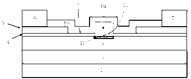
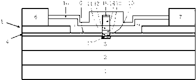
[0027] like image 3 As shown, the present invention relates to a gallium arsenide pseudomorphic high electron mobility transistor, comprising: a substrate 1, an AlGaAs buffer layer 2, a barrier layer 3, a low-doped GaAs layer 4, a highly doped GaAs layer 5, a source An electrode 6 and a drain electrode 7, a first groove 8 is provided between the source electrode 6 and the drain electrode 7, a second groove 10 is provided in the first groove 8, and a metal layer is arranged in the second groove 10. Specifically, the metal layer includes a first gate metal sublayer 11, a second gate metal sublayer 12, a third gate metal sublayer 13, a fourth gate metal sublayer 14, and a fifth gate metal sublayer 15. A barrier metal layer 17 is grown in the barrier layer 3.

[0028] In the present invention, the buffer layer 2 adopts the superlattice periodic structure of Al0.24Ga0.7...


PUM

PropertyMeasurementUnit
Thicknessaaaaaaaaaa
Thicknessaaaaaaaaaa
Thicknessaaaaaaaaaa

Abstract

The invention relates to a GaAs pseudomorphic high electron mobility transistor. The transistor comprises a substrate, an AlGaAs buffer layer, a barrier layer and a low GaAs doping layer, a high GaAs doping layer, a source electrode and a drain electrode. A first groove is provided between the source electrode and the drain electrode, a second groove is arranged in the first groove, and a metal layer is arranged in the second groove. The metal layer comprises a first gate metal sub-layer, a second gate metal sub-layer, a third gate metal sub-layer, a fourth gate metal sub-layer and a fifth gate metal sub-layer. A barrier metal layer is grown in the barrier layer. Compared with transistors in the prior art, the GaAs pseudomorphic high electron mobility transistor has the advantages that gate leakage currents can be inhibited, the gate drainage and the gate source breakdown voltage of the transistor can be improved, and the reliability of the GaAs transistor is improved; compared with common pure Pt gates, un-reacted Pt is larger in distance from the GaAs, so that the reliability of the GaAs enhanced transistor is further improved; and the contradiction between the technology with Pt as gate barriers and media assisted molded T-type gate technology can be well solved, and advantages of the T-type gate technology are fully developed.

Description

technical field [0001] The invention relates to a transistor and belongs to the technical field of semiconductor devices. Background technique [0002] Metal-semiconductor contact barriers in compound semiconductors have been extensively studied and their properties are well understood. Up to now, the selective application of metals in metal-semiconductor contact barriers has been basically completed. For example, Ti metal is used as the barrier contact metal in GaAs semiconductors. However, for GaN semiconductors that have emerged in recent years, Ti cannot be used as barrier metals. The reason is that the chemical properties of Ti and GaN semiconductors are unstable. It will react to generate other unstable products during use or even production process. Therefore, people use Pt metal to replace it. However, in the fabrication process of GaAs enhancement transistors, excessive Pt metal needs to be deposited to better control the distance between the gate metal and the ch...

Claims


Application Information

Patent Timeline
IPC IPC(8): H01L29/778H01L29/47
Inventor 章军云高建峰
Owner NO 55 INST CHINA ELECTRONIC SCI & TECHNOLOGYGROUP CO LTD
Learn More