
Compound semiconductor device and method of manufacturing same

A manufacturing method and semiconductor technology, applied in the direction of semiconductor/solid-state device manufacturing, semiconductor devices, electrical components, etc., can solve the problems of current collapse, reduce withstand voltage, leakage current, etc., and achieve the goal of suppressing gate leakage current and current collapse. Effect

Active Publication Date: 2012-06-06
FUJITSU LTD
View PDF5 Cites 1 Cited by
  • Summary
  • Abstract
  • Description
  • Claims
  • Application Information

AI Technical Summary

Problems solved by technology

[0010] However, Figure 1A The GaN-based HEMTs shown often have gate leakage or reduced withstand voltage
In addition, current collapse often occurs

Method used


Image

  • Compound semiconductor device and method of manufacturing same
  • Compound semiconductor device and method of manufacturing same
  • Compound semiconductor device and method of manufacturing same

Examples


Embodiment Construction

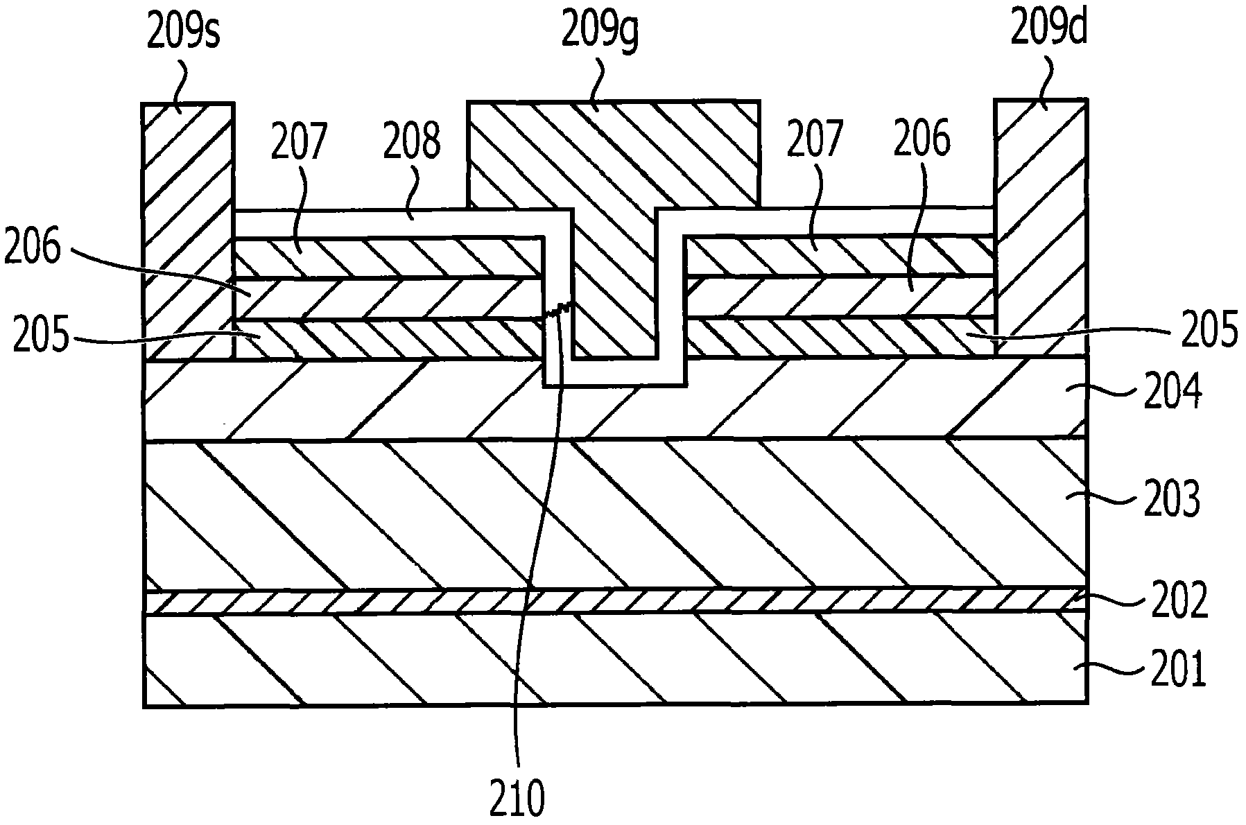
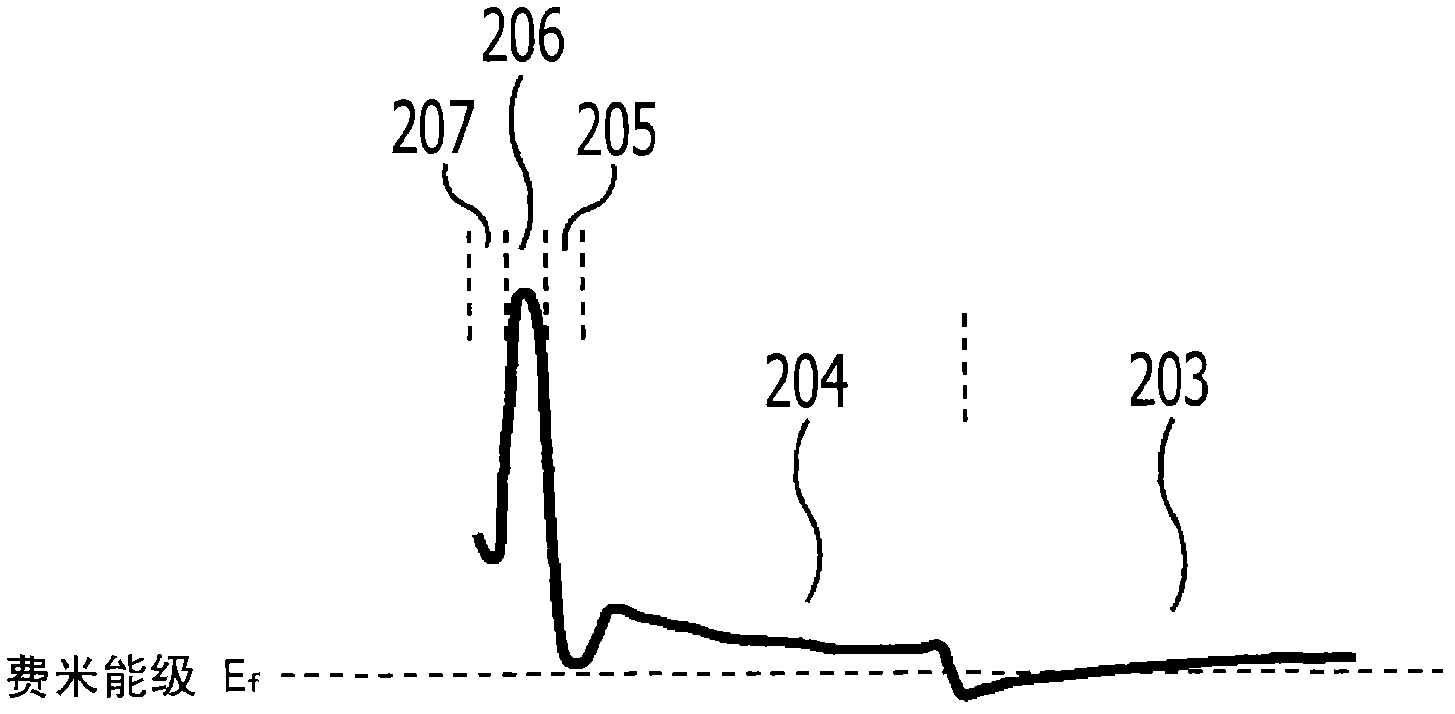
[0023] as previously stated and in Figure 1A The GaN-based HEMTs shown in often have gate leakage or reduced withstand voltage. In addition, current collapse often occurs. The inventors of the present invention have studied the cause Figure 1A The cause of gate leakage current or reduced withstand voltage in GaN-based HEMTs was shown, and the following findings were made. In GaN-based HEMTs, Figure 1B The conduction band shown is very close to the Fermi level near the interface between the i-AlN layer 206 and the n-GaN layer 205 . When a positive gate voltage is applied and the band moves down, a two-dimensional electron gas forms near this interface. Thus, if Figure 1A shown in Al 2 o 3 Dielectric breakdown 210 occurs in layer 208, resulting in gate leakage current or reduced withstand voltage.

[0024] The inventors of the present invention have also studied the cause Figure 1A The cause of current collapse in the GaN-based HEMT shown, and the following findings we...


PUM


Abstract

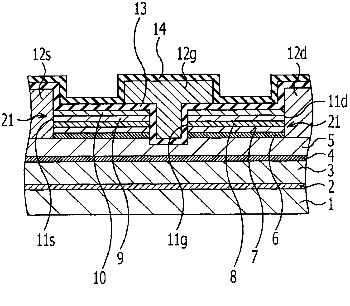
The present invention relates to a compound semiconductor device and a method of manufacturing the same. The compound semiconductor device includes: an electron transport layer formed over a substrate; an electron supply layer formed over the electron transport layer; and a cap layer formed over the electron supply layer; the cap layer includes a first compound semiconductor layer containing GaN; a second compound semiconductor layer containing AlN, which is formed over the first compound semiconductor layer; a third compound semiconductor layer containing GaN, which is formed over the second compound semiconductor layer; and at least one of a first AlGaN-containing layer and a second AlGaN-containing layer, with the first AlGaN-containing layer formed between the first compound semiconductor layer and the second compound semiconductor layer and the Al content increases toward the second compound semiconductor layer, and the second AlGaN-containing layer formed between the second compound semiconductor layer and the third compound semiconductor layer and the Al content increases toward the second compound semiconductor layer. The compound semiconductor device and the method can prevent the gate electrode current and the voltage from decreasing and / or inhibit current collapse.

Description

[0001] Related Application Cross Reference [0002] This application is based on and claims priority from a prior Japanese Patent Application No. 2010-269673 filed on December 2, 2010, the entire contents of which are hereby incorporated by reference. technical field [0003] The invention relates to a compound semiconductor device and a manufacturing method of the compound semiconductor device. Background technique [0004] A compound semiconductor device having a GaN layer and an AlGaN layer formed over a substrate, where the GaN layer is used as an electron transport layer, has been actively developed. An example of such a compound semiconductor device is a GaN-based high electron mobility transistor (HEMT). GaN-based HEMTs use a two-dimensional electron gas (2DEG) at a high concentration formed at the AlGaN / GaN heterojunction interface. [0005] GaN has a band gap (3.4eV) larger than Si (1.1eV) or GaAs (1.4eV). That is, GaN exhibits a higher breakdown field strength. ...

Claims


Application Information

Patent Timeline
IPC IPC(8): H01L29/778H01L21/335
CPCH01L29/7787H01L29/66462H01L29/2003H01L29/4236
Inventor 宫岛豊生吉川俊英今西健治多木俊裕金村雅仁
Owner FUJITSU LTD
Learn More