Epitaxial wafer of AlGaInP light emitting diode with sapphire underlay and preparation method thereof

A sapphire substrate and light-emitting diode technology, applied in the field of optoelectronics, can solve problems such as low luminous efficiency, achieve the effect of improving light output capability and reducing environmental pollution problems

Inactive Publication Date: 2009-09-23
Shandong Huaguang Optoelectronics Co. Ltd.
View PDF0 Cites 21 Cited by
  • Summary
  • Abstract
  • Description
  • Claims
  • Application Information

AI Technical Summary

Problems solved by technology

[0011] The invention aims at the problem of low luminous efficiency existing in the existing AlGaInP light-emitting diodes, and provides an AlGaInP light-emitting diode epitaxial wafer with a high luminous efficiency and a sapphire substrate and a preparation method thereof

Method used


Image

  • Epitaxial wafer of AlGaInP light emitting diode with sapphire underlay and preparation method thereof
  • Epitaxial wafer of AlGaInP light emitting diode with sapphire underlay and preparation method thereof

Examples


Embodiment 1

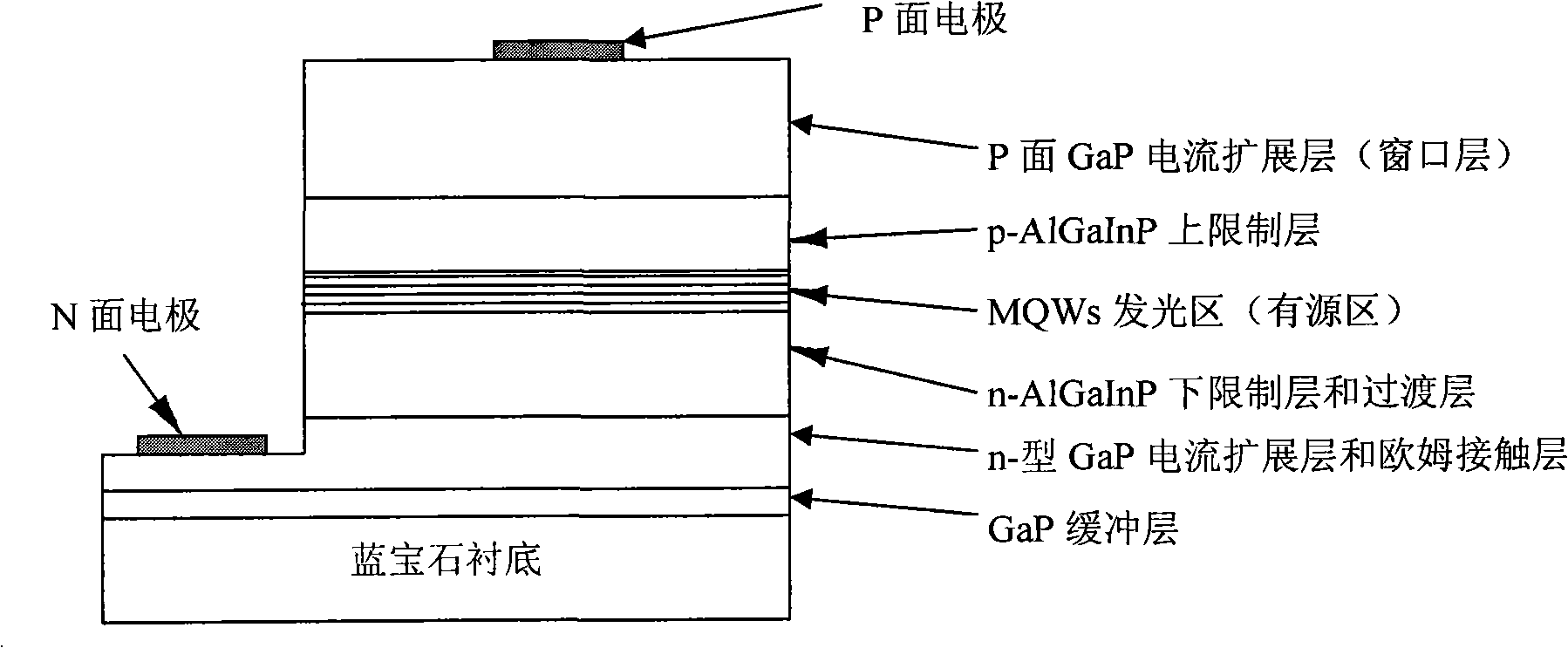
[0026] Such as figure 1 As shown, the AlGaInP light-emitting diode epitaxial wafer of the sapphire substrate of the present embodiment is a sapphire substrate, and its epitaxial structure is a GaP buffer layer (including two low-temperature GaP buffer layers and a high-temperature GaP buffer layer) on the sapphire substrate from bottom to top. layer combination), n-type GaP current spreading and ohmic contact layer, n-type AlGaInP transition and lower confinement layer, multiple quantum wells (MQWs) AlGaInP active region, p-type AlGaInP upper confinement layer and P-type current spreading layer. The P-face electrode (positive electrode) is made on the P-type current spreading layer by conventional die preparation technology, and the N-face electrode (negative electrode) is made on the n-type GaP current spreading and ohmic contact layer, so that the P-face electrode and the N-face electrode same above.

[0027]The preparation method of the AlGaInP light-emitting diode epitaxi...

Embodiment 2

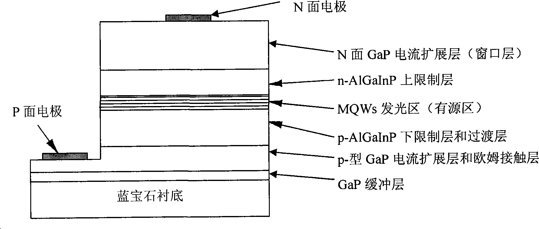
[0038] Such as figure 2 As shown, the epitaxial structure of the AlGaInP light-emitting diode epitaxial wafer on the sapphire substrate of this embodiment is a GaP buffer layer (including a combination of low-temperature GaP buffer layer and high-temperature GaP buffer layer) on the sapphire substrate from bottom to top, P-type GaP current expansion and ohmic contact layer, P-type AlGaInP transition and lower confinement layer, multiple quantum wells (MQWs) AlGaInP active region, n-type AlGaInP upper confinement layer, n-type GaP current expansion layer (window layer). The N-face electrode (negative electrode) is made on the n-type current spreading layer by conventional die preparation technology, and the P-face electrode (positive electrode) is made on the P-type GaP current spreading and ohmic contact layer, so that the P-face electrode and the N-face electrode same above.

[0039] The preparation method of the AlGaInP light-emitting diode epitaxial wafer of the above-men...


PUM


Abstract

The invention provides an epitaxial wafer of an AlGaInP light emitting diode with a sapphire underlay and a preparation method thereof. An epitaxial structure of the light emitting diode sequentically comprises the sapphire underlay, a low-temperature GaP buffer layer, a high-temperature GaP buffer layer, a GaP current expansion and ohmic contact layer, an AlGaInP transition layer, a lower limiting layer, a multiple quantum well AlGaInP active area, an AlGaInP upper limiting layer and a GaP current expansion layer from bottom to top. The preparation method comprises the steps that each epitaxial layer grows on the sapphire underlay layer by layer sequentially. The epitaxial wafer uses the sapphire as the epitaxial growth underlay and uses gallium phosphide as the buffer layer. Because the sapphire and the gallium phosphide material are transparent to a wave band from yellow to red, the problem of light absorption of the underlay does not exist. The gallium phosphide buffer layer can inhibit the material growth defect caused by lattice mismatch and heat expansion coefficient mismatch between the sapphire underlay and the AlGaInP material so as to greatly improve the light output capability of the light emitting diode.

Description

technical field [0001] The invention relates to an AlGaInP (aluminum gallium indium phosphide) light emitting diode (light emitting diode, LED) with a sapphire substrate and a preparation method thereof, belonging to the field of optoelectronic technology. Background technique [0002] Light-emitting diodes (LEDs) of different colors are prepared by different material systems. For yellow, orange, and red LEDs, the best performance is currently prepared by using AlGaInP material as the light-emitting layer. AlGaInP LEDs are grown on a GaAs (gallium arsenide) substrate, and its epitaxial material structure from bottom to top is GaAs substrate, GaAs buffer layer, n-type aluminum gallium indium phosphide [(Al x Ga 1-x ) 0.5 In 0.5 P] lower confinement layer, non-doped aluminum gallium indium phosphide [(Al x Ga 1-x ) 0.5 In 0.5 P / (Al y Ga 1-y ) 0.5 In 0.5 P](x≠y) light emitting region (also called active region), p-type aluminum gallium indium phosphide [(Al x Ga 1-...

Claims


Application Information

Patent Timeline
Patent Type & Authority Applications(China)
IPC IPC(8): H01L33/00
Inventor 李树强徐现刚张新马光宇任忠祥夏伟吴小强卢振于军吴作贵
Owner Shandong Huaguang Optoelectronics Co. Ltd.
Why Eureka
Try Eureka