Novel chip light source structure and preparation process thereof

A preparation process and light source technology, applied in the field of optoelectronics, can solve the problems of poor product index consistency, complex process, unfavorable environmental protection, etc., and achieve the effects of reducing production costs and cycle time, reducing environmental pollution, and improving light output capability.

Inactive Publication Date: 2018-11-06
SHENZHEN GUANGMAO ELECTRONICS
View PDF3 Cites 3 Cited by
  • Summary
  • Abstract
  • Description
  • Claims
  • Application Information

AI Technical Summary

Problems solved by technology

However, this method is complicated in process, the consistency of product indicators is not good, and a large amount of chemical waste liquid containing arsenic (As) is produced during the corrosion process, which needs further treatment, which is not good for environmental protection.

Method used


Image

  • Novel chip light source structure and preparation process thereof
  • Novel chip light source structure and preparation process thereof
  • Novel chip light source structure and preparation process thereof

Examples


Embodiment 1

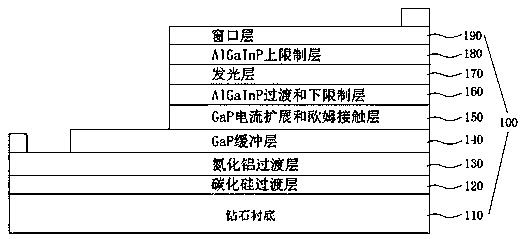
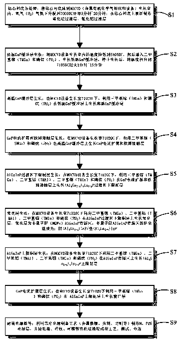
[0084] read on Figure 4 , the epitaxial structure includes from bottom to top a diamond substrate 110, a silicon carbide transition layer 120, an aluminum nitride transition layer 130, a low-temperature GaP buffer layer, a high-temperature GaP buffer layer, n-type GaP current spreading and ohmic contact layers 151, n Type AlGaInP transition and lower confinement layer 161, light emitting layer 170, p-type AlGaInP upper confinement layer 182, p-type window layer 192.

[0085] Further, the n-type AlGaInP transition and lower confinement layer 161 is provided with an N-face electrode layer 200, and the p-type window layer 192 is provided with a P-face electrode layer 300, so that the P-face electrode 300 and the N-face electrode 200 are simultaneously on the top.

[0086] In this specific embodiment, the diamond substrate 110 is made of a sapphire body rod, and the sapphire body is rod-shaped according to requirements, and the 2-inch or 4-inch rod is fixed, sliced, annealed, ch...

Embodiment 2

[0102] read on Figure 5 , the epitaxial structure 100 sequentially includes a diamond substrate 110, a silicon carbide transition layer 120, an aluminum nitride transition layer 130, a low-temperature GaP buffer layer, a high-temperature GaP buffer layer, a p-type GaP current extension and an ohmic contact layer 152 from bottom to top. , p-type AlGaInP transition and lower confinement layer 162, light emitting layer 170, n-type AlGaInP upper confinement layer 181, n-type window layer 191.

[0103] Further, the p-type AlGaInP transition and lower confinement layer 162 is provided with a P-face electrode layer 300, and the n-type window layer 191 is provided with an N-face electrode layer 200, so that the P-face electrode and the N-face electrode are on top .

[0104] In this specific embodiment, the diamond substrate 110 is made of a sapphire body rod, and the sapphire body is rod-shaped according to requirements, and the 2-inch or 4-inch rod is fixed, sliced, annealed, chamf...


PUM


Abstract

Disclosed is a novel chip light source structure; the novel chip light source structure comprises an epitaxial structure, an N surface electrode layer and a P surface electrode layer, wherein the epitaxial structure comprises a diamond substrate, a silicon carbide transition layer, an aluminum nitride transition layer, a GaP buffer layer, a GaP current expansion and ohmic contact layer, an AlGaInPtransition and lower limiting layer, a light-emitting layer, an AlGaInP upper limiting layer and a window layer which are sequentially arranged from the bottom up; the N surface electrode layer or the P surface electrode layer is arranged on the window layer; the N surface electrode layer or the P surface electrode layer is arranged on the GaP current expansion and ohmic contact layer; the diamond substrate is used as an epitaxial growth substrate, and the silicon carbide transition layer, the aluminum nitride transition layer and gallium phosphide are used as buffer layers, so that the problem of light absorption of the substrate is avoided, material growth defects caused by lattice mismatch and thermal expansion coefficient mismatch can be inhibited, the light output capability is greatly improved, and environmental pollution is reduced; and meanwhile, by adopting a molding organic silicon model particle forming process, the light color quality is high, the reliability is high, theprocess is optimized, and the cost is lowered.

Description

technical field [0001] The invention relates to the field of optoelectronics, in particular to a novel chip light source structure and a preparation process thereof. Background technique [0002] Light-emitting diodes of different colors are prepared by different material systems. For yellow, orange, and red light-emitting diodes, the best performance is now made of aluminum gallium indium phosphide materials, which are on GaAs (gallium arsenide) substrates grown, and its epitaxial material structure from bottom to top is GaAs substrate, GaAs buffer layer, n-type aluminum gallium indium phosphide [(Al x Ga 1-x ) 0.5 In 0.5 P] lower confinement layer, intrinsic aluminum gallium indium phosphide [(Al x Ga 1-x ) 0.5 In 0.5 P / (Al y Ga 1-y ) 0.5 In 0.5 P] (x¹y) light emitting region (also called active region), p-type aluminum gallium indium phosphide [(Al x Ga 1-x ) 0.5 In 0.5 P] upper confinement layer and p-type GaP (gallium phosphide) current spreading layer. ...

Claims


Application Information

Patent Timeline
Patent Type & Authority Applications(China)
IPC IPC(8): H01L33/02H01L33/12H01L33/56H01L21/02H01L33/00
CPCH01L33/02H01L21/02376H01L21/02447H01L21/02458H01L21/02502H01L21/02543H01L21/0262H01L33/0066H01L33/12H01L33/56H01L2933/005
Inventor 李锋吉爱华叶浩文
Owner SHENZHEN GUANGMAO ELECTRONICS
Why Eureka
Try Eureka