A kind of SMT tin adding device and tin adding method

A technology of soldering and soldering layers, which is applied in the direction of assembling printed circuits, printed circuits, and electrical components with electrical components. Effect

Active Publication Date: 2021-08-31
QIKU INTERNET TECH SHENZHEN CO LTD
View PDF14 Cites 0 Cited by
  • Summary
  • Abstract
  • Description
  • Claims
  • Application Information

AI Technical Summary

Problems solved by technology

[0004] The inventors of this application have found in the long-term research and development process that the thickened steel mesh can be used to increase the thickness of the solder paste, but after printing the solder paste, it is difficult to release the thickened steel mesh

Method used


Image

  • A kind of SMT tin adding device and tin adding method
  • A kind of SMT tin adding device and tin adding method
  • A kind of SMT tin adding device and tin adding method

Examples


Embodiment Construction

[0027] The application will be described in further detail below in conjunction with the accompanying drawings and embodiments. In particular, the following examples are only used to illustrate the present application, but not to limit the scope of the present application. Likewise, the following embodiments are only some of the embodiments of the present application but not all of them, and all other embodiments obtained by those skilled in the art without creative efforts fall within the protection scope of the present application.

[0028] The orientation or positional relationship indicated by the terms "inner" and "outer" in the specification and claims of the application and the above drawings are based on the orientation or positional relationship shown in the drawings, or the usual placement of the product in use. The orientation or positional relationship is only for the convenience of describing this application and simplifying the description, and does not indicate ...


PUM

PropertyMeasurementUnit
thicknessaaaaaaaaaa

Abstract

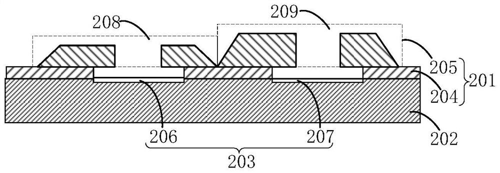
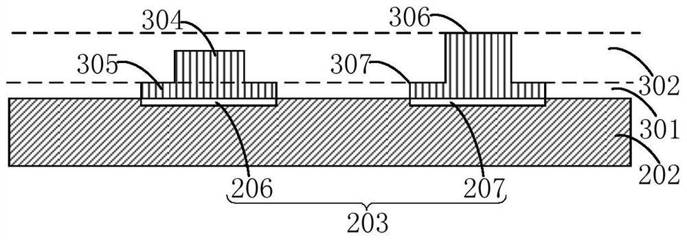
The application discloses an SMT tinning device and a tinning method. The tinning device is used to print solder on the pads of the PCB board, and the tinning device at least includes: a first steel mesh, the first steel mesh is arranged on the first surface of the PCB board, the first steel mesh is provided with solder The first opening corresponding to the pad, the solder layer is set on the pad through the first stencil; the second stencil is set on the first stencil, and the second stencil is provided with a second opening corresponding to the first opening , the thickened solder layer is disposed on the solder layer through the second stencil; wherein, the area of ​​the second opening is smaller than or equal to the area of ​​the first opening. In this way, while increasing the amount of solder on the pad, the efficiency and effect of the stencil release can be ensured.

Description

technical field [0001] The present application relates to the field of surface mount technology (Surface Mount Technology, SMT), in particular to an SMT tinning device and a tinning method. Background technique [0002] SMT reflow soldering is one of the main methods of soldering printed circuit boards (PCB boards). It is an inevitable trend for the development of electronic products in the direction of miniaturization, and printing solder paste is one of the important processes in SMT reflow soldering. 1. Printing solder paste is to leak the paste-like solder paste to the corresponding pad of the PCB through the openings on the stencil. [0003] The existing bottom screen used for SMT reflow soldering adopts a stencil with a thickness of about 0.13mm or 0.15mm, and the thickness of the solder paste after the stencil is demoulded can only reach 0.18mm and 0.20mm. [0004] The inventors of the present application have discovered in the long-term research and development proc...

Claims


Application Information

Patent Timeline
Patent Type & Authority Patents(China)
IPC IPC(8): H05K3/34
CPCH05K3/3494H05K2203/0126
Inventor 李帅
Owner QIKU INTERNET TECH SHENZHEN CO LTD
Why Eureka
Try Eureka