

Ceramic electronic component and manufacturing method of the same
- Summary
- Abstract
- Description
- Claims
- Application Information
AI Technical Summary
Benefits of technology
Problems solved by technology
Method used
Image

Examples
first embodiment
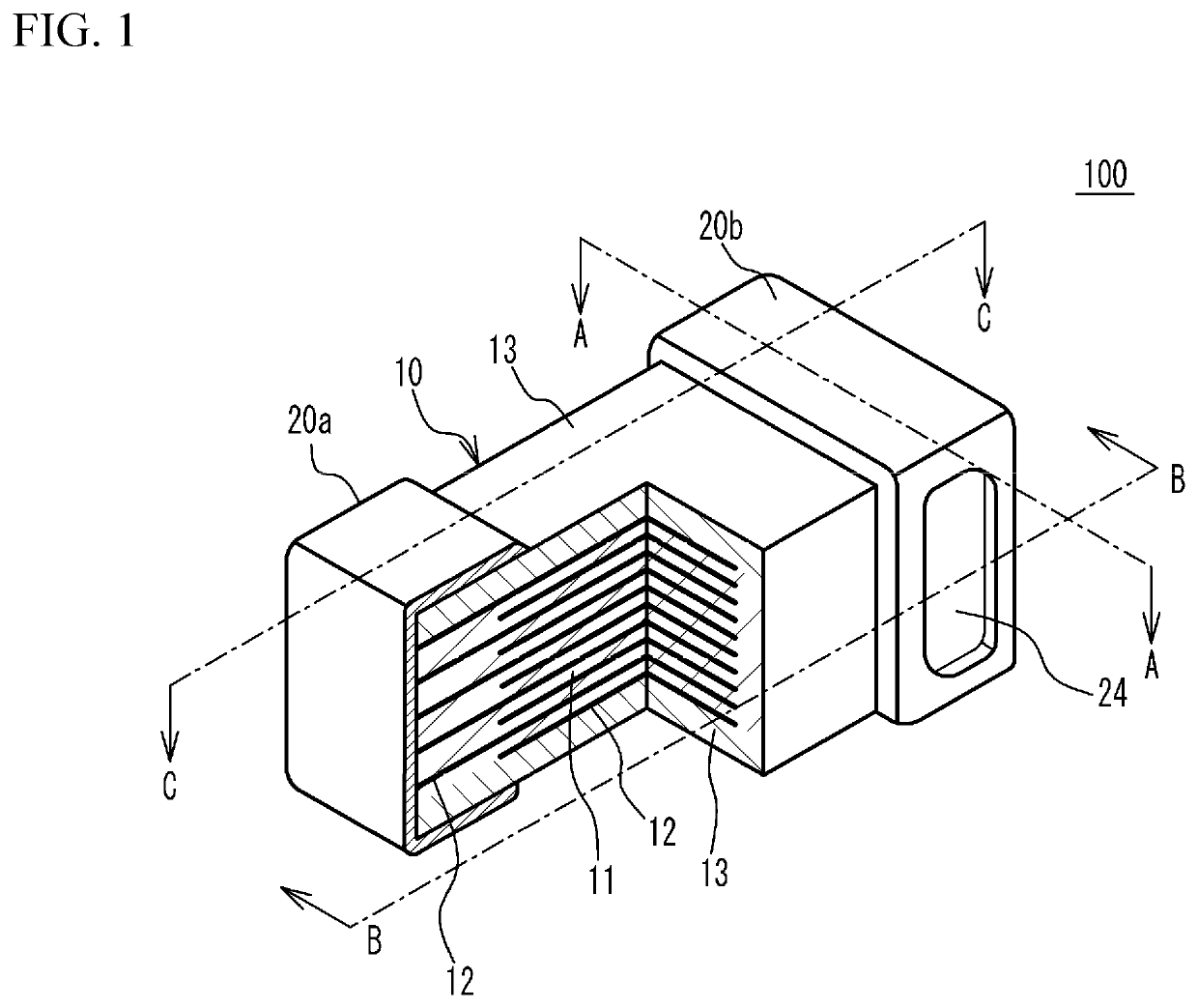
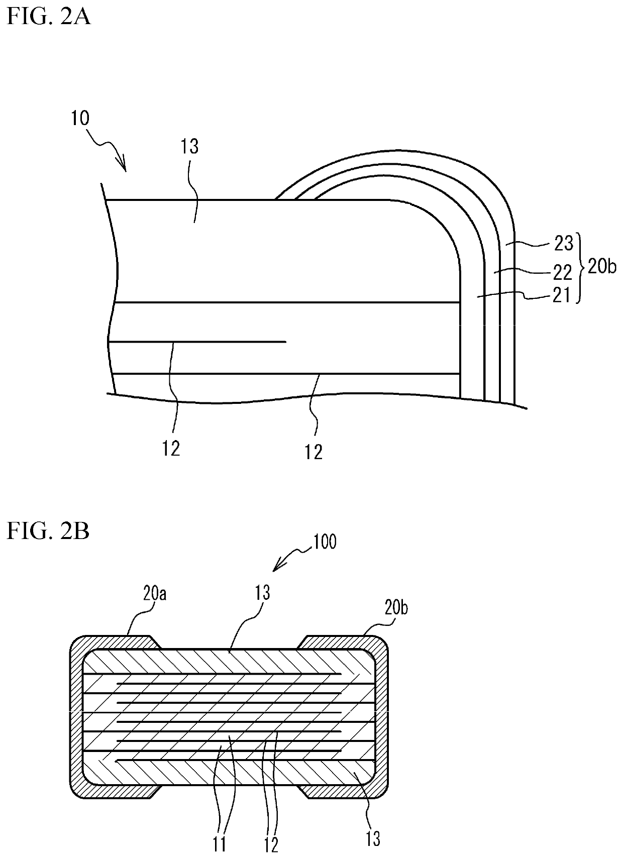
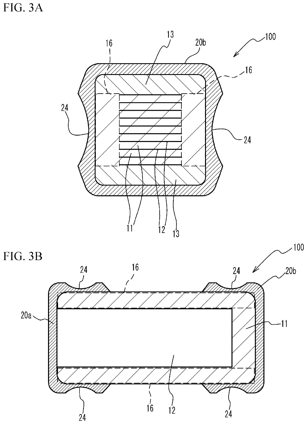
[0030]First, a multilayer ceramic capacitor will be described. FIG. 1 is a partial cross-sectional perspective view of a multilayer ceramic capacitor 100 in accordance with a first embodiment. As illustrated in FIG. 1, the multilayer ceramic capacitor 100 includes a multilayer chip 10 having a rectangular parallelepiped shape, and external electrodes 20a and 20b respectively provided on two edge faces of the multilayer chip 10 facing each other. The four faces other than the two edge faces of the multilayer chip 10 will be referred to as side faces. The external electrodes 20a and 20b extend to four side faces. However, the external electrodes 20a and 20b are spaced from each other on each of the four side faces.
[0031]The multilayer chip 10 has a structure designed to have dielectric layers 11 and internal electrode layers 12 alternately stacked. The dielectric layer 11 contains a ceramic material acting as a dielectric material. End edges of the internal electrode layers 12 are alt...
second embodiment
[0054]FIG. 8 is a partial cross-sectional perspective view of a multilayer ceramic capacitor 100A in accordance with a second embodiment. FIG. 9A is a cross-sectional view taken along line A-A in FIG. 8, and FIG. 9B is a cross-sectional view taken along line C-C in FIG. 8.
[0055]The multilayer ceramic capacitor 100A differs from the multilayer ceramic capacitor 100 (see FIG. 1) in that the recessed portion 24 is formed on at least one of the two side faces facing each other in the stack direction (the top face and the bottom face in the stack direction) among four side faces of the multilayer chip 10, and no recessed portion 24 is formed on the remaining two side faces. Note that no recessed portion 24 means that the recess level X described in the first embodiment is less than 25%.
[0056]As illustrated in FIG. 9A, in the multilayer ceramic capacitor 100A, each of the two side faces facing each other in the stack direction is formed of the cover layer 13 and the side margin portions 1...
examples
[0075]The multilayer ceramic capacitors in accordance with the embodiment were fabricated, and the variation in the recess level X was examined.
PUM
| Property | Measurement | Unit |
|---|---|---|
| Fraction | aaaaa | aaaaa |
| Fraction | aaaaa | aaaaa |
| Density | aaaaa | aaaaa |
Abstract
Description
Claims
Application Information