Light-emitting diode package

a technology of light-emitting diodes and led tubes, which is applied in the direction of basic electric elements, electrical apparatus, and semiconductor devices, can solve the problems of reducing hindering insufficient bonding strength of the silver glue, so as to enhance the efficiency of the led device, enhance the reliability of the led package, and increase the bonding strength

Inactive Publication Date: 2011-05-05
SEMILEDS OPTOELECTRONICS CO LTD +1
View PDF16 Cites 23 Cited by
  • Summary
  • Abstract
  • Description
  • Claims
  • Application Information

AI Technical Summary

Benefits of technology

[0008]A light-emitting diode (LED) package is provided, whereby reliability of the LED package is enhanced through higher bonding strength...

Problems solved by technology

However, the bonding strength provided by the silver glue is often insufficient, wherein the LED chip detaches from the lead frame, thereby decreasing reliability of the ...

Method used


Image

  • Light-emitting diode package
  • Light-emitting diode package
  • Light-emitting diode package

Examples


Embodiment Construction

[0016]The following description is of the best-contemplated mode of carrying out the invention. This description is made for the purpose of illustrating the general principles of the invention and should not be taken in a limiting sense. The scope of the invention is best determined by reference to the appended claims.

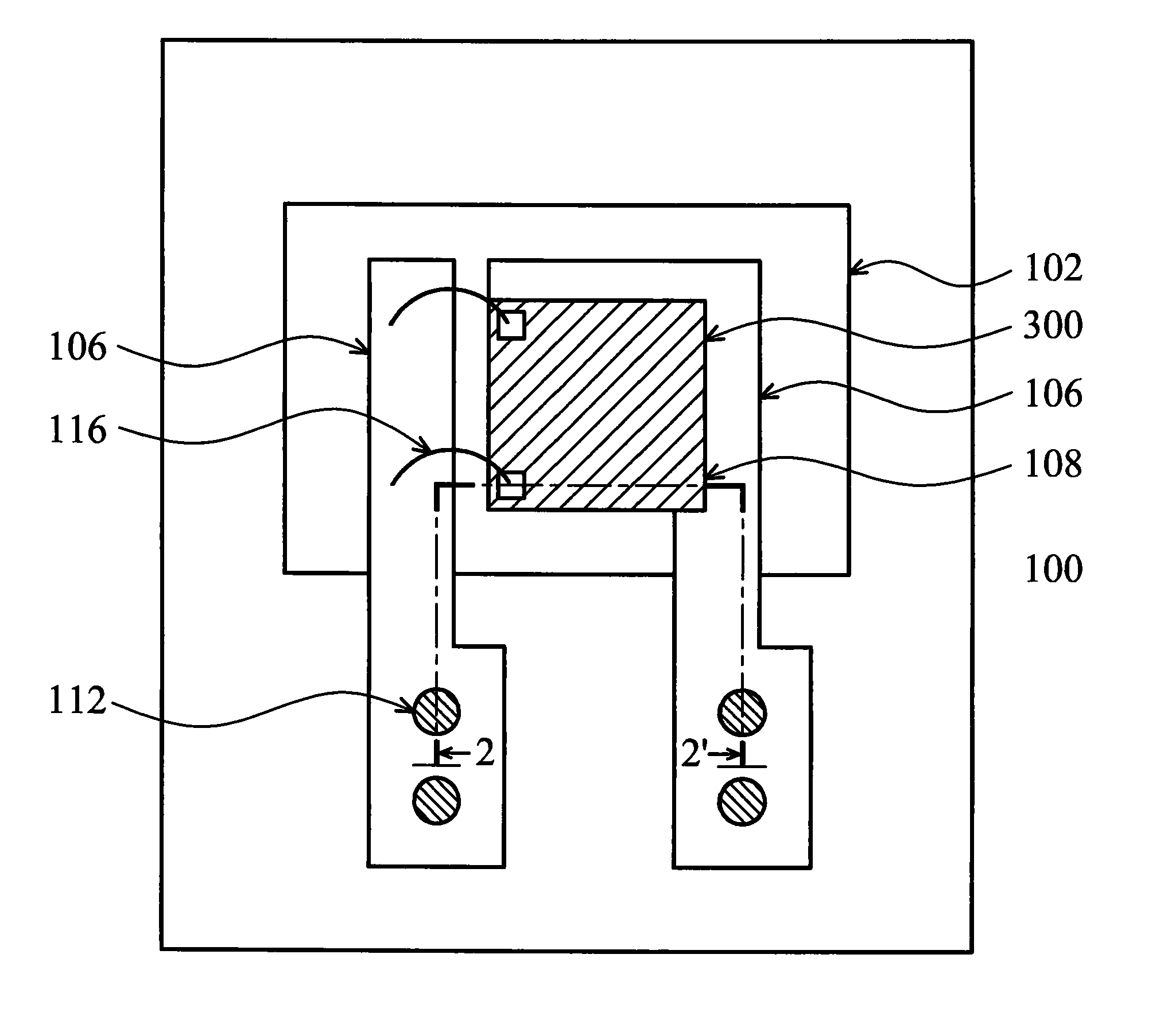
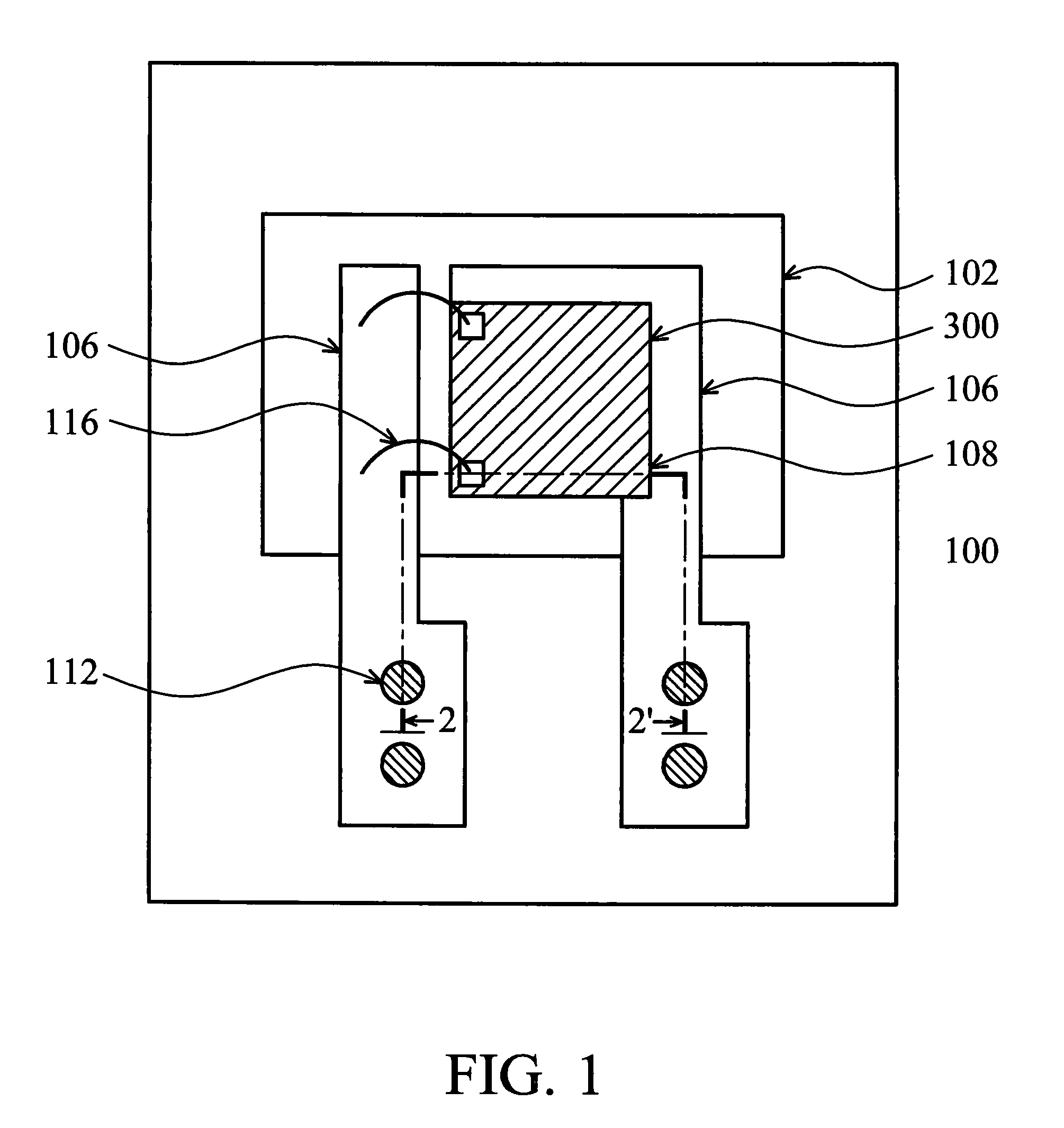
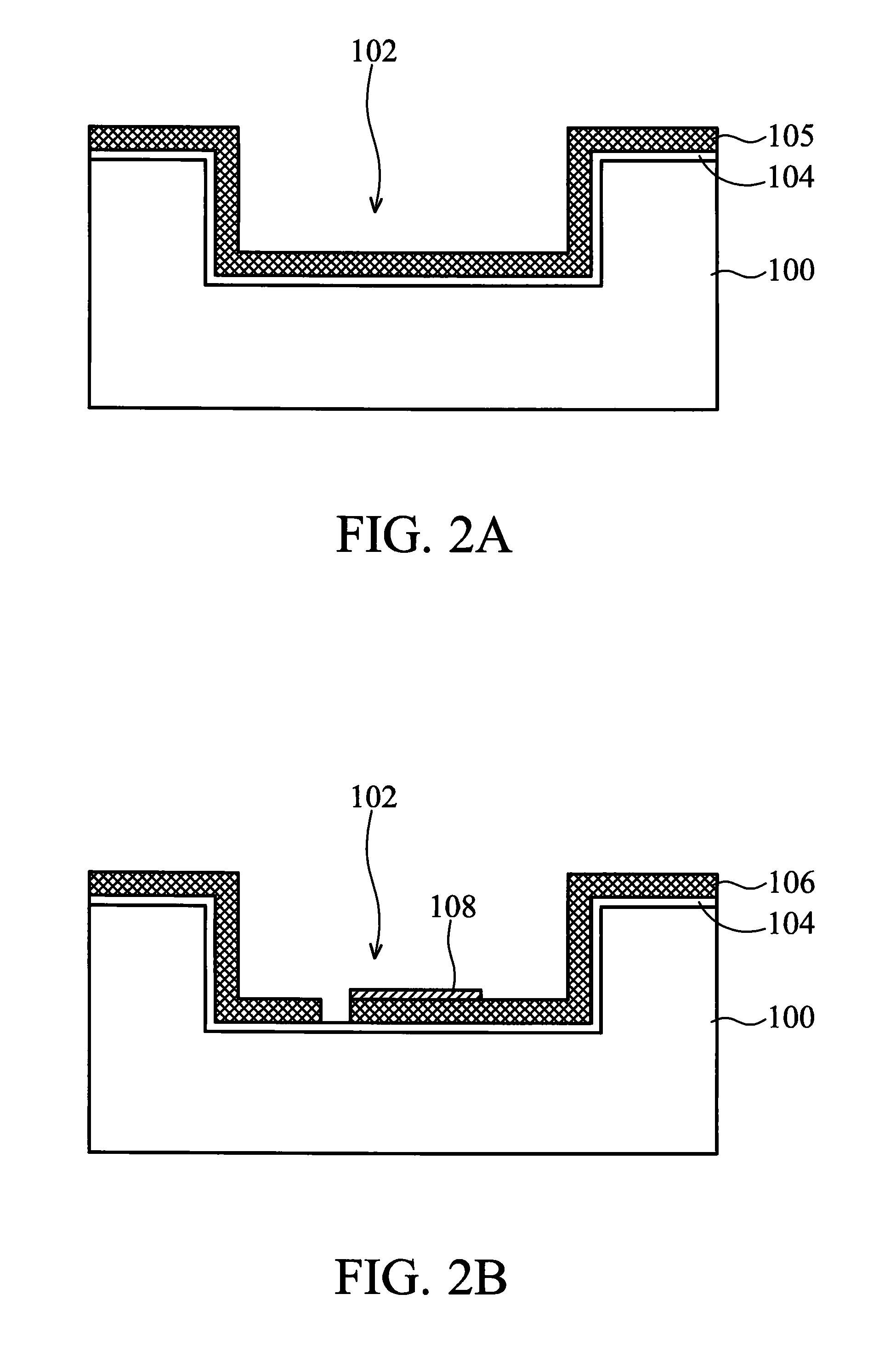
[0017]The invention provides LED packages with high bonding strength between a substrate and an LED chip thereof, with high heat dissipating efficiency. FIG. 1 shows a plane view of an LED package according to an embodiment of the invention. As shown in FIG. 1, a light-emitting diode chip 300 is disposed in a cavity 102 of a substrate 100. In an embodiment of the invention, the light-emitting diode chip 300 may be a vertical typed LED chip, having a lower contact (not shown) such as a p-type contact on a bottom surface of the LED chip 300 and an upper contact 210 such as an n-type contact on a top surface of the LED chip 300. In another embodiment, the lower contact of...


PUM


Abstract

A light-emitting diode package is provided. The light-emitting diode package comprises a substrate and a first metal layer disposed over the substrate. A solder layer is disposed on the first metal layer and a light-emitting diode chip is disposed on the solder layer, wherein the light-emitting diode chip comprises a conductive substrate and a multilayered epitaxial structure formed on the conductive substrate, and wherein the conductive substrate is adjacent to the solder layer.

Description

BACKGROUND OF THE INVENTION[0001]1. Field of the Invention[0002]The invention relates to a light-emitting diode (LED) package and more particularly to an LED package with improved bonding strength between a substrate and an LED chip thereof.[0003]2. Description of the Related Art[0004]Light-emitting diodes (LEDs) are playing an increasingly important role in the daily lives of humans. They are capable of reliably providing illumination with high brightness and thus are applied in display devices, traffic lights, indicator units and other electronic devices. LEDs are fabricated by depositing an n-doped semiconductor layer, an active layer and a p-doped semiconductor layer on a substrate. Some LEDs have an n-contact formed on one side of a device and a p-contact formed on the opposite side of the device. Other LEDs have both contacts formed on the same side of a device.[0005]In conventional packaging methods, LED chips are packaged by a lead frame packaging technology. The LED chip is...

Claims


Application Information

Patent Timeline
IPC IPC(8): H01L33/00
CPCH01L24/32H01L24/48H01L24/49H01L24/83H01L24/85H01L33/486H01L33/62H01L2224/05554H01L2224/2612H01L2224/29111H01L2224/32225H01L2224/48091H01L2224/48227H01L2224/49113H01L2224/73265H01L2224/83815H01L2224/85439H01L2224/85444H01L2224/92247H01L2924/00014H01L2924/01004H01L2924/01006H01L2924/01013H01L2924/01024H01L2924/01029H01L2924/01033H01L2924/01042H01L2924/01047H01L2924/01049H01L2924/0105H01L2924/01073H01L2924/01074H01L2924/01075H01L2924/01078H01L2924/01079H01L2924/01082H01L2924/0132H01L2924/01322H01L2924/014H01L2924/12041H01L2924/15153H01L2924/157H01L2924/15747H01L2924/15787H01L2924/1579H01L2924/00012H01L2924/00H01L2924/00015H01L2224/45099H01L2224/45015H01L2924/207
Inventor CHANG, KUO-CHINGKUO, WU-CHENGLIN, TZU-HAN
Owner SEMILEDS OPTOELECTRONICS CO LTD
Why Eureka
Try Eureka