

Production method of multilayer ceramic electronic device
a production method and ceramic technology, applied in the manufacture of capacitors, fixed capacitor details, fixed capacitors, etc., can solve the problems of inability to achieve a larger capacity, disadvantages below, and spheroidizing of internal electrode layers, so as to prevent cracks and prevent spheroidization , the effect of preventing cracks
- Summary
- Abstract
- Description
- Claims
- Application Information
AI Technical Summary
Benefits of technology
Problems solved by technology
Method used
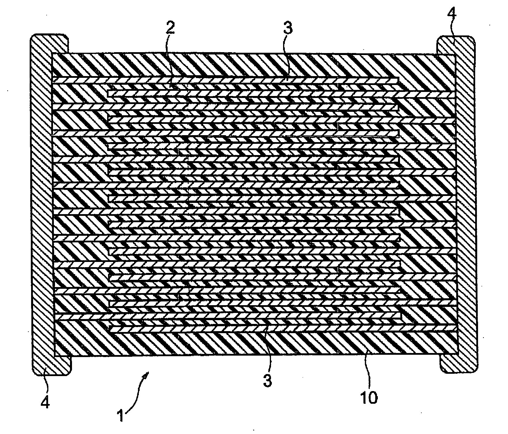
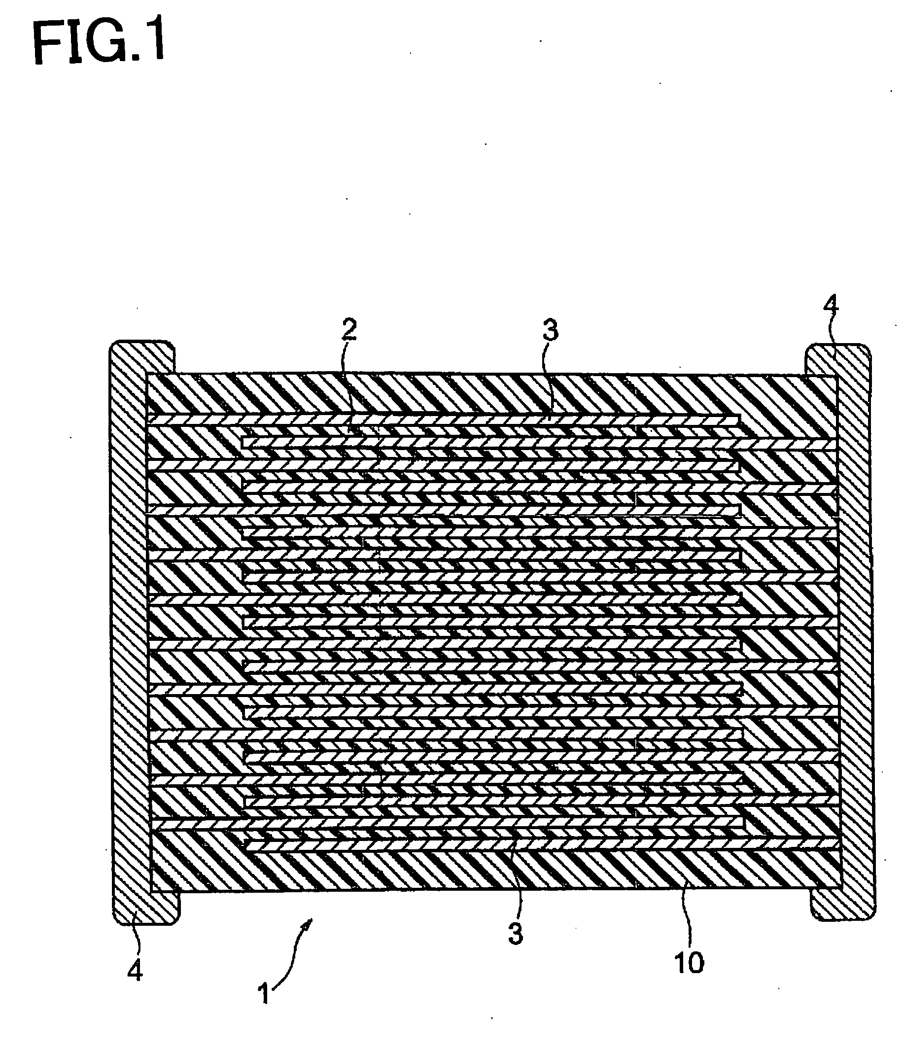
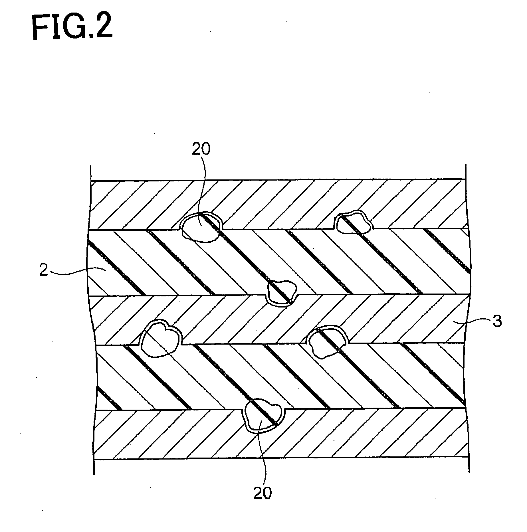
Image

Examples
example 1
[0083] First, as starting materials for producing a dielectric material, (BaTiO3) as a main component material and Y2O3, V2O5, CrO, MgO, SiO2 and CaO as subcomponent materials having an average particle diameter of 0.2 μm were prepared. Next, the prepared starting materials were wet mixed by a ball mill for 16 hours to fabricate a dielectric material.
[0084] The dielectric material fabricated as above in an amount of 100 parts by weight, an acrylic resin in an amount of 4.8 parts by weight, ethyl acetate in an amount of 100 parts by weight, mineral spirit in an amount of 6 parts by weight and toluene in an amount of 4 parts by weight were mixed by a ball mill to form paste, so that dielectric layer paste was obtained.
[0085] Next, Ni particles having an average particle diameter of 0.2 μm in an amount of 100 parts by weight, BaTiO3 (an average particle diameter: 0.05 μm) as a first common material in an amount of 20 parts by weight, BaTiO3 (an average particle diameter: 0.5 μm) as a...
example 2
[0110] Other than using Ni powder having an average particle diameter of 0.1 μm as the Ni powder included in the conductive material paste and changing a content of the second common material as shown in Table 2, multilayer ceramic capacitor samples were produced in the same way as in the example 1 and the evaluation was made in the same way as in the example 1. The results are shown in Table 2.
TABLE 2Multilayer Ceramic Capacitor SampleSecondCommonMaterialParticleConductive Material PasteDiameter / Crack ArisingShort-VoltageFirst CommonSecond CommonThicknessInternalRateCircuitResistanceNiMaterialMaterialof InternalElectrode(ppm)CapacitanceDefect RateDefect RateSamplePowder(parts by(parts byElectrodeLayer1000 ppm(%)(%)(%)No.(μm)(μm)weight)(μm)weight)Layer (μm)Thicknessor lowerwithin −10%50% or lower50% or lower120.10.0520—01.00.50870000812130.10.05200.511.00.5060000−11013140.10.05200.531.00.50900−21016150.10.05200.551.00.50100−51516160.10.05200.5131.00.500−52120170.10.05200.5151.00.5...
example 3
[0112] Other than changing a ratio of the first common material included in the conductive material paste as shown in Table 3, multilayer ceramic capacitor samples were produced in the same way as in the sample No. 6 in example 1, and evaluation was made in the same way as in the example 1. The results are shown in Table 3.
TABLE 3Multilayer Ceramic Capacitor SampleSecondCommonMaterialParticleConductive Material PasteDiameter / Crack ArisingShort-VoltageFirst CommonSecond CommonThicknessInternalRateCircuitResistanceNiMaterialMaterialof InternalElectrode(ppm)CapacitanceDefect RateDefect RateSamplePowder(parts by(parts byElectrodeLayer1000 ppm(%)(%)(%)No.(μm)(μm)weight)(μm)weight)Layer (μm)Thicknessor lowerwithin −10%50% or lower50% or lower180.2—00.551.00.502000−152024190.20.0540.551.00.501400−111820200.20.0550.551.00.50700−9202060.20.05200.551.00.500−53032210.20.05350.551.00.50800−102430220.20.05400.551.00.503000−122532
[0113] From Table 3, in the sample No. 18 not including the first...
PUM
| Property | Measurement | Unit |
|---|---|---|
| particle diameter | aaaaa | aaaaa |
| thickness | aaaaa | aaaaa |
| particle diameter | aaaaa | aaaaa |
Abstract
Description
Claims
Application Information