Chip mounting method

a chip and mounting method technology, applied in the field of chip mounting methods, can solve the problems of reducing the reliability of electrical bonding between the bump and the electrode of the substrate, and affecting the reliability of the electrical bonding

Inactive Publication Date: 2004-09-28
TORAY ENG CO LTD
View PDF12 Cites 24 Cited by
  • Summary
  • Abstract
  • Description
  • Claims
  • Application Information

AI Technical Summary

Benefits of technology

In the chip mounting method according to the present invention, it is preferred that the underfill agent is expanded up to a side portion of the chip by further pushing the chip toward the substrate together with heating the bump or electrode or after the heating. Particularly, it is preferred that a fillet is formed at the side portion of the chip by the underfill agent expanded up to the side portion of the chip. By such an underfill agent expanded sufficiently broad, the bonding strength between the chip and the substrate can be increased as well as a desired excellent electrical insulation can be ensured.
In the above-described chip mounting method according to the present invention, the underfill agent is applied before chip mounting, and before heating, the applied underfill agent is expanded so as to bury therein the bump and the electrode of the substrate in contact with each other, and therefore, when the bump is heated and molten, the bump is cut off from the surrounding atmosphere by the underfill agent, and the secondary oxidation of the bump can be prevented. Therefore, the purging due to nitrogen gas and the like for preventing the secondary oxidation such as a conventional method becomes unnecessary, and the apparatus and the process can be greatly simplified.
This chip mounting method according to the present invention is not a method for injecting an underfill agent into a gap between a chip and a substrate after preliminarily bonding a bump and an electrode and thereafter mainly bonding them by heating as in a conventional method, but a method for expanding an underfill agent to around a bump of chip and an electrode of a substrate in contact with each other, and performing a main bonding at a time without performing a preliminary bonding by heating the bump or the electrode in the expanded underfill agent. Because this bonding is carried out through heating and melting of the bump or the electrode in the underfill agent which does not come into contact with oxygen, as mentioned above, there is no fear that the secondary oxidation occurs by heating. Besides, during this heating and melting, re-flow necessary for the bump or the electrode is carried out at the same time. Therefore, in the method according to the present invention, the mounting is completed substantially by two processes of the primary oxidation preventing treatment process and the heating and bonding process of the chip and the substrate including the application of the underfill agent, thereby greatly reducing the number of the processes for chip mounting and greatly simplifying both the process and the apparatus.
Furthermore, if the underfill agent is expanded up to the side portion of the chip by further pushing the chip toward the substrate after the bump or the electrode is softened or molten by heating, the bonding strength and the retaining strength of the chip relative to the substrate can be increased. Especially, if the underfill agent is expanded so as that a fillet can be formed on the side portion of the chip, by forming the fillet, invasion of moisture and the like into a portion between the chip and the substrate can be prevented by the underfill agent forming the fillet in addition to the underfill agent present between the chip and the substrate, and at the same time, it becomes possible to increase the retaining strength and the bonding strength of the chip. Further, because a fear that the underfill agent remains between the bump and the electrode can be removed by the above-described pushing, a more stable electric connection can be achieved therebetween.
Thus, in the chip mounting method according to the present invention, a secondary oxidation of the bump bonding portion can be prevented without using nitrogen gas and the like as in a conventional method, both the apparatus and the process can be greatly simplified, and a chip mounting having a high reliability in bonding and insulation properties can be carried out inexpensively.

Problems solved by technology

In such a conventional chip mounting method, however, when the solder bump is heated and molten in the preliminary bonding process of the chip and the substrate, there is a fear that the bonded portion is secondarily oxidized by the surrounding atmosphere.
If such a secondary oxidation occurs, it may decrease the reliability of the electrical bonding between the bump and the electrode of the substrate.
However, such purging by nitrogen gas and the like causes a chip mounting apparatus to become large-sized, the mounting apparatus and the mounting process to become complicated, and the cost thereof to increase, and because it is necessary to take a time for the purging by nitrogen gas and the like, a high-speed mounting may be obstructed.
Further, in the above-described conventional mounting method, because it is necessary to apply a flux and remove the flux by cleaning after the bonding for melt-bonding of the solder bump, there is a problem that the number of processes until completion of main bonding is fairly large.
Moreover, the perfect cleaning of the flux is difficult, and therefore, the residual components may reduce the reliability of the bonding.
However, in this method, basically only the cleaning process of the flux becomes unnecessary, and the method is poor in effect for reducing the number of the processes in the bonding.
Further, in this method, as the bump pitch has been in a fine pitch condition, it has become difficult to inject the underfill agent.
Further, if the aforementioned primary oxidation preventing treatment is carried out, the application of flux becomes unnecessary, and a further simplification becomes possible.

Method used


Image

  • Chip mounting method
  • Chip mounting method

Examples


Embodiment Construction

Hereinafter, desirable embodiments of the present invention will be explained referring to figures.

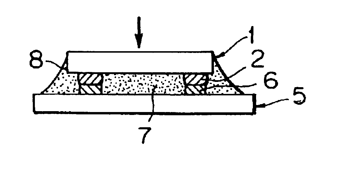
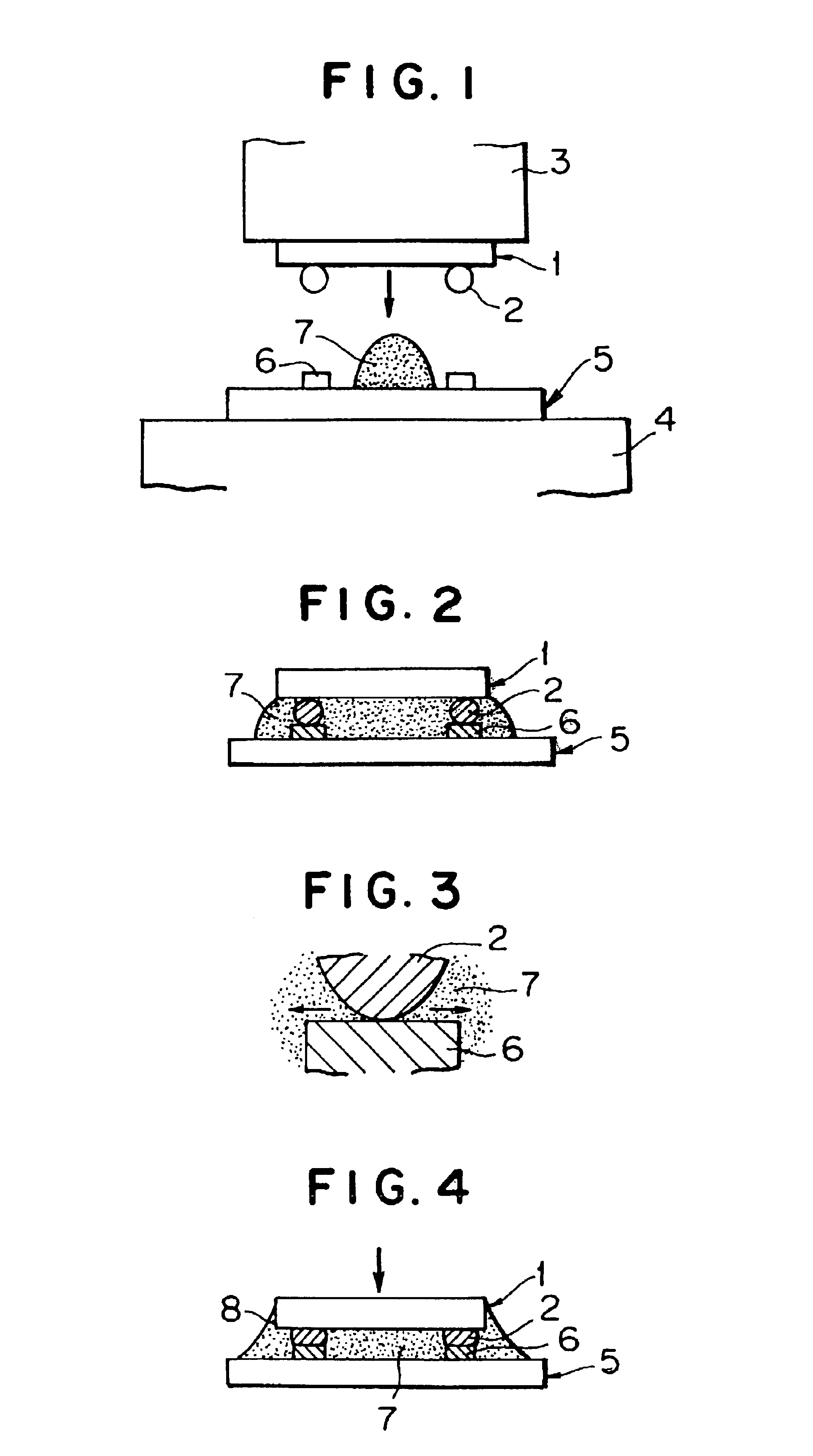
FIG. 1 shows a state immediately before chip mounting in a chip mounting method according to an embodiment of the present invention, and shows a case where bumps are formed on the chip side and electrodes are formed on the substrate side. In FIG. 1, numeral 1 shows a chip (for example, an IC chip), and at positions corresponding to the positions of electrodes (not shown) provided on the lower surface of the chip, bumps 2 (in this embodiment, solder bumps) are formed. Chip 1 is held by suction on the lower surface of a heat tool 3 of a chip bonding machine. In this embodiment, a primary oxidation preventing treatment such as the aforementioned treatment is performed to the surfaces of at least one of bumps 2 and electrodes of a substrate, and the solder bonding can be carried out without applying a flux.

As the primary oxidation preventing treatment for bumps 2 or the electrodes, the afo...


PUM

PropertyMeasurementUnit
total bonding strengthaaaaaaaaaa
speedaaaaaaaaaa
melting pointaaaaaaaaaa

Abstract

A method for mounting a chip on a substrate includes applying the underfill agent onto at least one of the substrate and the chip and moving the chip to the substrate to bring the bump into contact with the electrode. The method also includes steps to distribute the underfill agent in a space between the chip and the substrate, to around the bump and the electrode, heating the bump or electrode in the state that the bump is buried in the underfill agent to melt the bump or electrode so as to weld the bump to the electrode.

Description

The present invention relates to a method for mounting a chip, and specifically to a chip mounting method for mounting a chip directly onto a substrate in a form of face down and performing underfill between the chip and the substrate.BACKGROUND ART OF THE INVENTIONA chip mounting method is well known, wherein a bump is formed on a chip by a solder and the like, the chip is approached to a substrate in a form of face down, and after the bump is brought into contact with an electrode of the substrate, the bump of the chip is heated and molten to be bonded to the electrode of the substrate. An underfill agent, which is composed of a nonconductive adhesive, is injected into a gap between the chip and the substrate in order to increase the total bonding strength between the chip and the substrate. Further, the reliability of the electrical insulation between the bonded portions is increased by a condition where the underfill agent is filled around the bump of the chip and the electrode ...

Claims


Application Information

Patent Timeline
Patent Type & Authority Patents(United States)
IPC IPC(8): H01L21/56H01L21/02
CPCH01L21/563H01L24/29Y10T29/4913H01L2224/73203H01L2224/73204H01L2224/83192H01L2924/01005H01L2924/01018H01L2924/01033H01L2924/01075H01L2924/01078H01L2924/01079H01L2924/14H01L2924/01006H01L2224/16225H01L2924/12042H01L2924/00014H01L24/81H01L2224/32225H01L2924/00H01L2224/0401H01L21/60
Inventor YAMAUCHI, AKIRA
Owner TORAY ENG CO LTD
Why Eureka
Try Eureka