Semiconductor device and method for manufacturing semiconductor device

a semiconductor and semiconductor technology, applied in the direction of semiconductor devices, basic electric elements, electrical equipment, etc., can solve the problems of high cost, high cost, and high cost of semiconductor epitaxial layer cracks, and achieve the effect of bonding strength

Active Publication Date: 2010-06-24
STANLEY ELECTRIC CO LTD
View PDF1 Cites 23 Cited by
  • Summary
  • Abstract
  • Description
  • Claims
  • Application Information

AI Technical Summary

Benefits of technology

[0021]In accordance with the method for manufacturing a semiconductor device of the present invention, it is possible to obtain a bonding strength that is high enough for natural removal or separation of the growth substrate not to occur between the growth substrate and the semiconductor epitaxial layer. On the other hand, a growth substrate can be removed without using LLO in the growth substrate removal step.

Problems solved by technology

When separating or removing the growth substrate using the LLO method, the nitride semiconductor decomposes and produces N2 gas by absorbing laser light, and there are cases in which the gas pressure produces cracks in the semiconductor epitaxial layer.
The implementation of the LLO method leads to higher costs because expensive special equipment therefore must be used.
It is furthermore difficult to process a plurality of wafers in a single process using the LLO method, and the process entails scanning a laser light across the entire wafer surface.
Therefore, a relatively long processing time is required.
Second, the growth substrate must not be naturally separated.
Specifically, post-processing becomes difficult when the growth substrate is naturally separated during handling of the wafer or in an intermediate process step because the thickness of the semiconductor epitaxial layer is small.
For example, electrode formation and bonding with the support substrate becomes very difficult when the growth substrate is separated due to thermal shock or the like in the epitaxial growth step of the semiconductor layer.

Method used


Image

  • Semiconductor device and method for manufacturing semiconductor device
  • Semiconductor device and method for manufacturing semiconductor device
  • Semiconductor device and method for manufacturing semiconductor device

Examples


Embodiment Construction

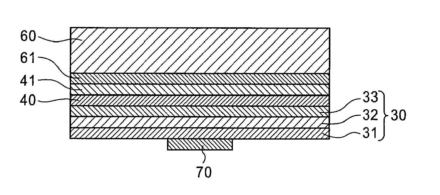
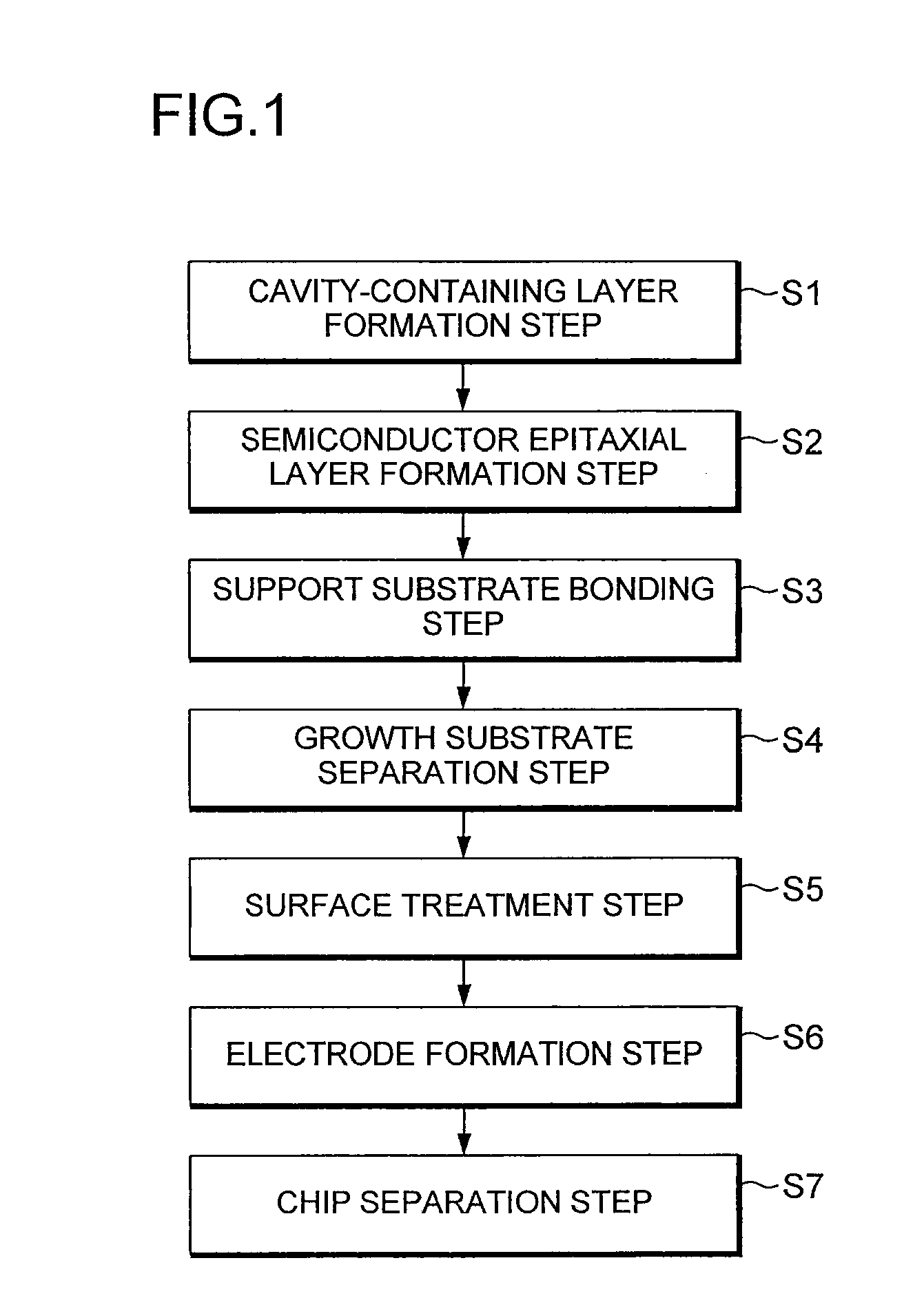
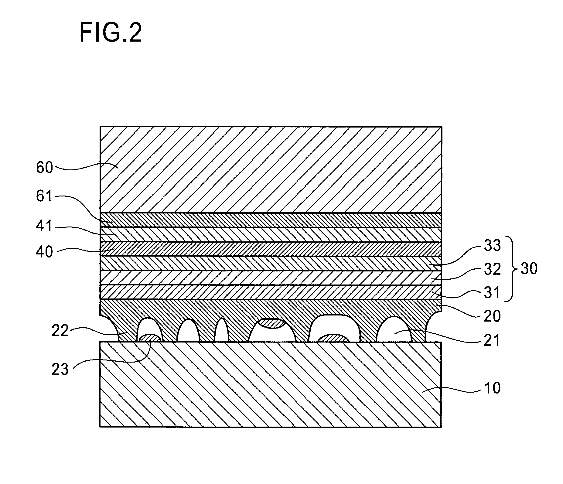
[0030]Embodiments of the present invention are described below with reference to the drawings. In the drawings shown below, the same reference numerals are used for the essentially the same or equivalent constituent elements and portions. The present invention relates to a semiconductor device, and a semiconductor light-emitting device is described as an example below. FIG. 1 is a flowchart of the steps of manufacturing a semiconductor light-emitting device according to an embodiment of the present invention. FIG. 2 is a cross-sectional view showing the structure of the semiconductor light-emitting diode in the step prior to removal of the growth substrate.

[0031]The method for manufacturing a semiconductor light-emitting device of the present embodiment includes a cavity-containing layer formation step (step S1) of forming a cavity-containing layer 20 composed of a group III nitride having numerous internal cavities on the growth substrate 10; a semiconductor epitaxial layer formati...


PUM


Abstract

A cavity-containing layer having a plurality of cavities is formed on a growth substrate by carrying out in alternating fashion a plurality of cycles of a first and second growth steps of growing a group III nitride at growth rates different from each other. The semiconductor epitaxial layer is subsequently formed on the cavity-containing layer, after which a support substrate is bonded to the semiconductor epitaxial layer. The growth substrate is separated from the cavity-containing layer.

Description

BACKGROUND OF THE INVENTION[0001]1. Field of the Invention[0002]The present invention relates to a semiconductor device and a method for manufacturing a semiconductor device.[0003]2. Description of the Related Art[0004]Light-emitting diodes and other semiconductor light-emitting devices are manufactured by forming semiconductor layers or layered structure including an n-layer, an active layer, a p-layer on a growth substrate such as a sapphire substrate, and forming electrodes on the growth substrate and the surface of the semiconductor layer. Part of the semiconductor layer is etched away using reactive ion etching or another technique to expose the n-layer and form electrodes on the n-layer and p-layer, respectively.[0005]Semiconductor light-emitting devices are increasingly efficient and have higher output through recent technological advances. However, the amount of heat produced in the semiconductor light-emitting devices has also increased together with the higher output, whic...

Claims


Application Information

Patent Timeline
Patent Type & Authority Applications(United States)
IPC IPC(8): H01L29/20H01L21/18
CPCH01L21/0242H01L21/02458H01L21/0254H01L33/0079H01L21/02636H01L33/007H01L21/0262H01L33/0093
Inventor CHINONE, TAKAKOLIANG, JI-HAOSHIBATA, YASUYUKIHIGASHINO, JIRO
Owner STANLEY ELECTRIC CO LTD
Why Eureka
Try Eureka